
25L12835F Datasheet – 128Mb bits serial Flash memory
128Mb bits serial Flash memory, which is configured as 16,777,216 x 8 internally.
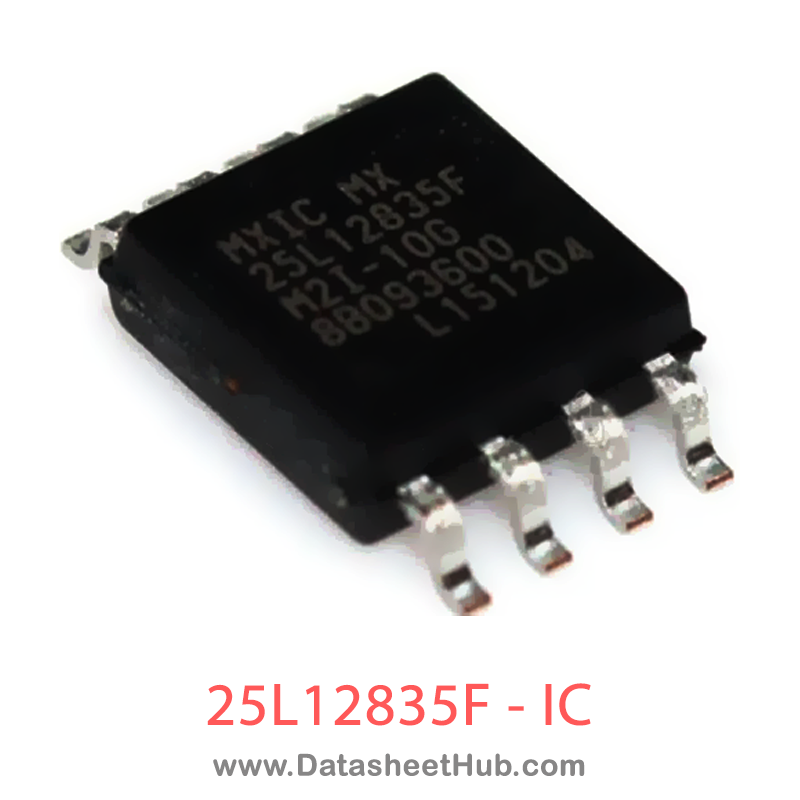
25L12835F, 25L12835F overview
The 25L12835F, 25L12835F is a 128Mb bits serial Flash memory, which is configured as 16,777,216 x 8 internally., supplied in these packages: 8-pin SOP(200mil), 16-pin SOP(300mil), 8-land WSON (6x5mm), 8-land WSON (8x6mm). The absolute maximum ratings table on this page lists the 5 limits from the manufacturer's datasheet that must not be exceeded. This page brings together the 25L12835F, 25L12835F pinout and maximum ratings, with the full datasheet PDF to preview below or download.
MX25L12835F is 128Mb bits serial Flash memory, which is configured as 16,777,216 x 8 internally. When it is in two or four I/O mode, the structure becomes 67,108,864 bits x 2 or 33,554,432 bits x 4. MX25L12835F feature a serial peripheral interface and software protocol allowing operation on a simple 3-wire bus while it is in single I/O mode. The three bus signals are a clock input (SCLK), a serial data input (SI), and a serial data output (SO). Serial access to the device is enabled by CS# input.
When it is in two I/O read mode, the SI pin and SO pin become SIO0 pin and SIO1 pin for address/dummy bits in- put and data output. When it is in four I/O read mode, the SI pin, SO pin, WP# and RESET# pin become SIO0 pin, SIO1 pin, SIO2 pin and SIO3 pin for address/dummy bits input and data output.
The MX25L12835F MXSMIOâ (Serial Multi I/O) provides sequential read operation on whole chip.
After program/erase command is issued, auto program/erase algorithms which program/erase and verify the speci- fied page or sector/block locations will be executed. Program command is executed on byte basis, or page (256 bytes) basis, or word basis for erase command is executed on sector (4K-byte), block (32K-byte), or block (64K-byte), or whole chip basis.
To provide user with ease of interface, a status register is included to indicate the status of the chip. The status read command can be issued to detect completion status of a program or erase operation via WIP bit.
Advanced security features enhance the protection and security functions, please see security features section for more details.
When the device is not in operation and CS# is high, it is put in standby mode. The MX25L12835F utilizes Macronix's proprietary memory cell, which reliably stores memory contents even after 100,000 program and erase cycles.
Datasheet
25L12835F, 25L12835F features
- GENERAL
- Serial Peripheral Interface compatible -- Mode 0 and Mode 3
- Single Power Supply Operation
- - 2.7 to 3.6 volt for read, erase, and program operations
- 128Mb: 134,217,728 x 1 bit structure or 67,108,864 x 2 bits (two I/O mode) structure or 33,554,432 x 4 bits (four I/O mode) structure
- Protocol Support Single I/O, Dual I/O and Quad I/O
- Single I/O, Dual I/O and Quad I/O
- Latch-up protected to 100mA from -1V to Vcc +1V
- Low Vcc write inhibit is from 2.3V to 2.5V
- Fast read for SPI mode
- Support clock frequency up to 133MHz for all protocols
- Support Fast Read, 2READ, DREAD, 4READ, QREAD instructions.
- Configurable dummy cycle number for fast read operation
- Quad Peripheral Interface (QPI) available
- Equal Sectors with 4K byte each, or Equal Blocks with 32K byte each or Equal Blocks with 64K byte each Any Block can be erased individually
- Any Block can be erased individually
- Programming
- 256byte page buffer
- Quad Input/Output page program (4PP) to enhance program performance
- Typical 100,000 erase/program cycles
- 20 years data retention
- SOFTWARE FEATURES
- Input Data Format 1-byte Command code
- 1-byte Command code
- Advanced Security Features Block lock protection
- Block lock protection
- The BP0-BP3 and T/B status bit defines the size of the area to be protection against program and erase instruc- tions
- Advanced sector protection function (Solid and Password Protect)
- Additional 4K bit security OTP
- Features unique identifier
- factory locked identifiable, and customer lockable
- Command Reset
- Program/Erase Suspend and Resume operation
- Electronic Identification
- JEDEC 1-byte manufacturer ID and 2-byte device ID
- RES command for 1-byte Device ID
- REMS command for 1-byte manufacturer ID and 1-byte device ID
- Support Serial Flash Discoverable Parameters (SFDP) mode
- HARDWARE FEATURES SCLK Input Serial clock input SI/SIO0 Serial Data Input or Serial Data Input/Output for 2 x I/O read mode and 4 x I/O read mode SO/SIO1 Serial Data Output or Serial Data Input/Output for 2 x I/O read mode and 4 x I/O read mode WP#/SIO2 Hardware write protection or serial data Input/Output for 4 x I/O read mode RESET#/SIO3 Hardware Reset pin or Serial input & Output for 4 x I/O re
- SCLK Input Serial clock input
25L12835F, 25L12835F pinout

| Name | Description |
|---|---|
| CS# | Chip Select |
| SI/SIO0 | Serial Data Input (for 1 x I/O)/ Serial Data Input & Output (for 2xI/O or 4xI/O read mode) |
| SO/SIO1 | Serial Data Output (for 1 x I/O)/ Serial Data Input & Output (for 2xI/O or 4xI/O read mode) |
| SCLK | Clock Input |
| WP#/SIO2 | Write protection: connect to GND or Serial Data Input & Output (for 4xI/O read mode) |
| RESET#/SIO3 | Hardware Reset Pin Active low or Serial Data Input & Output (for 4xI/O read mode) |
| VCC | + 3V Power Supply |
| GND | Ground |
| NC | No Connection |
| DNU | Do not use |
Absolute maximum ratings
| Parameter | Value |
|---|---|
| Ambient Operating Temperature | Industrial grade |
| Storage Temperature | -65°C to 150°C |
| Applied Input Voltage | -0.5V to VCC+0.5V |
| Applied Output Voltage | -0.5V to VCC+0.5V |
| VCC to Ground Potential | -0.5V to 4.0V |
25L12835F, 25L12835F applications
- Flash Memory Storage
- Microcontroller Program Storage
- Firmware Updates
- Consumer Electronics
- Networking Equipment
Comments 0
Leave a comment