
H9TP32A4GDBCPR Datasheet – 4GB eNAND (x8) Flash Memory
4GB eNAND (x8) / LPDDR2-S4B 4Gb(x32) / Flash Memory
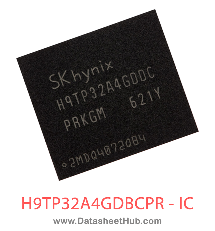
H9TP32A4GDBCPR overview
The H9TP32A4GDBCPR is a 4GB eNAND (x8) / LPDDR2-S4B 4Gb(x32) / Flash Memory, supplied in these packages: 162-ball FBGA – 11.5×13.0mm2, 1.0t, 0.5mm pitch. The absolute maximum ratings table on this page lists the 6 limits from the manufacturer's datasheet that must not be exceeded. This page brings together the H9TP32A4GDBCPR maximum ratings, with the full datasheet PDF to preview below or download.
The SK hynix e‐NAND is an embedded flash memory storage solution. The SK hynix e‐NAND was developed for universal low cost data storage and communication media. The SK hynix e‐NAND is fully compatible with MMC bus and host.
The SK hynix e‐NAND communications are made through an advanced 13‐pin bus, and it can be either 1‐bit, 4‐bit, or 8‐bit in width. The SK hynix e‐NAND operates in high‐speed mode at clock frequencies equal or higher than 20MHz as defined in the MMC JEDEC standard. The communication protocol is defined in this MMC JEDEC standard.
The SK hynix e‐NAND is designed to cover a wide area of applications such as smart phones, cameras, organizers, PDA, digi‐ tal recorders, MP3 players, pagers, electronic toys, etc. Features are mainly high speed performance, low power consump‐ tion, low cost and high density.
To meet the requirements of embedded high density storage media and mobile applications, the SK hynix e‐NAND supports 3.3V for VCC, and 3.3V/1.8V for VCCQ. The address argument for the SK hynix e‐NAND is consistent with the sector (512‐byte sectors) instead of the byte. This means that the SK hynix e‐NAND is not capable to support backward compatibility for devices with the condition of the density with lower than 2 Gigabytes. If the SK hynix e‐NAND receives the byte addressing type, then the SK hynix e‐NAND will change its state to inactive. The SK hynix e‐NAND has the built‐in intelligent controller which manages interface protocols, data storage and retrieval, wear leveling, bad block management, garbage collection, and internal ECC. The SK hynix e‐NAND protects the data con‐ tents from the host sudden power off failure by safe‐update operations with reliable write features. The device supports a boot operation with enhance area and sleep/awake commands. In particular, the host power regulator for VCC can minimize the power consumption during the sleep state.
Datasheet
H9TP32A4GDBCPR features
- [CI-MCP ]
- Operation Temperature (-25) oC ~ 85oC
- (-25) oC ~ 85oC
- Package 162-ball FBGA - 11.5x13.0mm2, 1.0t, 0.5mm pitch Lead & Halogen Free
- 162-ball FBGA - 11.5x13.0mm2, 1.0t, 0.5mm pitch
- Lead & Halogen Free
- [ e-NAND ]
- Packaged NAND flash memory with Multi Media-Card interface
- e-NAND system specification, compliant withV4.41
- Full backward compatibility with previous e-NAND system specification
- Bus mode
- High-speed eMMC protocol.
- Three different data bus widths:1 bit, 4 bits,8 bits.
- Data transfer rate: up to 104Mbyte/s
- DDR mode supported
- Operating voltage range: VCCQ = 3.3/1.8V VCC = 3.3V
- VCCQ = 3.3/1.8V
- VCC = 3.3V
- Error free memory access
- Internal error correction code
- Internal enhanced data managementalgorithm (Wear levelling, Bad blockmanagement, Garbage collection)
- Possibility for the host to make sudden powerfailure safe-update operations for data content
- Security
- Password protection of data
- Secure Erase
- Secure Trim
- Secure bad block management
- Write Protection
- Boot Normal / Alternative boot sequence method
- Normal / Alternative boot sequence method
- Power saving Enhanced power saving method byintroducing sleep functionality
- Enhanced power saving method byintroducing sleep functionality
- Partition management with enhanced storage.
- Hardware reset supported
- [ LPDDR2 S4B ]
- VDD1 = 1.8V (1.7V to 1.95V)
- VDD2, VDDCA and VDDQ = 1.2V (1.14V to 1.30)
- HSUL_12 interface (High Speed Unterminated Logic 1.2V)
- Double data rate architecture for command, address anddata Bus; all control and address except CS_n, CKE latched at bothrising and falling edge of the clock CS_n, CKE latched at rising edge of the clock two data accesses per clock cycle
- all control and address except CS_n, CKE latched at bothrising and falling edge of the clock
Absolute maximum ratings
| Parameter | Symbol | Value | Unit |
|---|---|---|---|
| Voltage on VDD1 relative to VSS | VDD1 | Rating -0.4 ~ 2.3 / Notes 1 | V |
| Voltage on VDD2 relative to VSS | VDD2 | Rating -0.4 ~ 1.6 / Notes 1 | V |
| Voltage on VDDCA relative to VSSCA | VDDCA | Rating -0.4 ~ 1.6 / Notes 1, 3 | V |
| Voltage on VDDQ relative to VSSQ | VDDQ | Rating -0.4 ~ 1.6 / Notes 1, 2 | V |
| Voltage on Any Pin relative to VSS | VIN, VOUT | Rating -0.4 ~ 1.6 | V |
| Storage Temperature | TSTG | Rating -55 ~ 125 / Notes 4 | oC |
H9TP32A4GDBCPR applications
- NAND Flash Memory
- Solid-State Drives (SSDs)
- Embedded Systems
- Data Storage Solutions
- Mobile Devices
Comments 0
Leave a comment