

SAF7741HV Datasheet – Audio Digital Signal Processor
Dual IF car radio and audio DSP (N1F)
SAF7741HV overview
The 9-bit video input processor is a combination of a
two-channel analog preprocessing circuit including source selection, anti-aliasing filter and ADC, an automatic clamp and gain control, a Clock Generation Circuit (CGC), a digital multi-standard decoder (PAL BGHI, PAL M, PAL N, combination PAL N, NTSC M, NTSC-Japan, NTSC N and SECAM), a brightness, contrast and saturation control circuit, a multi-standard VBI data slicer and a 27 MHz VBI data bypass; see Fig.1.
The pure 3.3 V CMOS circuit SAF7113H, analog front-end and digital video decoder, is a highly integrated circuit for desktop video applications. The decoder is based on the principle of line-locked clock decoding and is able to decode the colour of PAL, SECAM and NTSC signals into ITU-R BT.601 compatible colour component values. The SAF7113H accepts as analog inputs CVBS or S-video (Y/C) from TV or VTR sources. The circuit is I2C-bus controlled.
The integrated high performance multi-standard data slicer supports several VBI data standards:
- Teletext [WST (World Standard Teletext), CCST (Chinese teletext)] (625 lines)
- Teletext [US-WST, NABTS (North-American Broadcast Text System) and MOJI (Japanese teletext)] (525 lines)
- Closed caption [Europe, US (line 21)]
- Wide Screen Signalling (WSS)
- Video Programming Signal (VPS)
- Time codes (VITC EBU/SMPTE)
- High-speed VBI data bypass for inter cast application.
| Part Number | SAF7741HV |
| Function | Dual IF car radio and audio DSP (N1F) |
| Package | HLQFP144 Type |
| Manufacturer | Philips, NXP |
| Datasheet | Download PDF  |

Datasheet
SAF7741HV features
- Four analog inputs, internal analog source selectors,
- e.g. 4 ´ CVBS or 2 ´ Y/C or (1 ´ Y/C and 2 ´ CVBS)
- Two analog preprocessing channels in differential CMOS style for best S/N-performance
- Fully programmable static gain or automatic gain control for the selected CVBS or Y/C channel
- Switchable white peak control
- Two built-in analog anti-aliasing filters
- Two 9-bit video CMOS Analog-to-Digital Converters (ADCs), digitized CVBS or Y/C-signals are available on the VPO-port via I2C-bus control
- On-chip clock generator
- Line-locked system clock frequencies
- Digital PLL for horizontal sync processing and clock generation, horizontal and vertical sync detection
- Requires only one crystal (24.576 MHz) for all standards
- Automatic detection of 50 and 60 Hz field frequency, and automatic switching between PAL and NTSC standards
- Luminance and chrominance signal processing for PAL BGHI, PAL N, combination PAL N, PAL M, NTSC M, NTSC N, NTSC 4.43, NTSC-Japan and SECAM
- User programmable luminance peaking or aperture correction
- Cross-colour reduction for NTSC by chrominance comb filtering
- PAL delay line for correcting PAL phase errors
- Brightness Contrast Saturation (BCS) and hue control on-chip
- Real-time status information output (RTCO)
- Two multi functional real-time output pins controlled by I2C-bus
- Multi-standard VBI-data slicer decoding World Standard Teletext (WST), North-American Broadcast Text System (NABTS), closed caption, Wide Screen Signalling (WSS), Video Programming System (VPS), Vertical Interval Time Code (VITC) variants (EBU/SMPTE) etc.
- Standard ITU 656 YUV4:2:2 format (8-bit) on VPO output bus
- Enhanced ITU 656 output format on VPO output bus containing
- active video
- raw CVBS data for INTERCAST applications (27 MHz data rate)
- decoded VBI data
- Boundary scan test circuit complies with the “IEEE Std. 1149.b1 - 1994” (ID-Code = 1 7113 02B)
- I2C-bus controlled (full read-back ability by an external controller, bit rate up to 400 kbits/s)
- Low power (<0.5 W), low voltage (3.3 V), small package (QFP44)
- Power saving mode by chip enable input
- Detection of copy protected input signals according to the macrovision standard. Can be used to prevent unauthorized recording of pay-TV or video tape signals.
SAF7741HV pinout
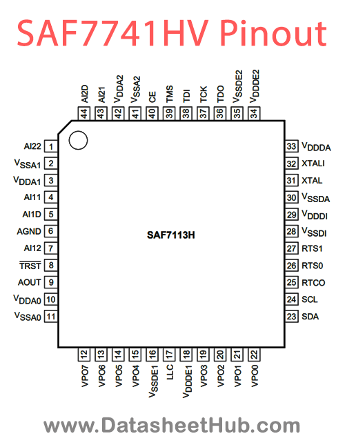
| Pin | Name | Description |
|---|---|---|
| 1 | AI22 | analog input 22 |
| 2 | VSSA1 | ground for analog supply voltage channel 1 |
| 3 | VDDA1 | positive supply voltage for analog channel 1 (+3.3 V) |
| 4 | AI11 | analog input 11 |
| 5 | AI1D | differential analog input for AI11 and AI12; has to be connected to ground via a capacitor; see application diagram of Fig.31 |
| 6 | AGND | analog signal ground connection |
| 7 | AI12 | analog input 12 |
| 8 | TRST | test reset input (active LOW), for boundary scan test; notes 1, 2 and 3 |
| 9 | AOUT | analog test output; for testing the analog input channels, 75 W termination possible |
| 10 | VDDA0 | positive supply voltage (+3.3 V) for internal Clock Generation Circuit (CGC) |
| 11 | VSSA0 | ground for internal clock generation circuit |
| 12 to 15 | VPO7 to VPO4 | digital VPO-bus output signal; higher bits of the 8-bit output bus. The output data types of the VPO-bus are controlled via I2C-bus registers LCR2 to LCR24; see Table 4. If I2C-bus bit VIPB = 1, the higher bits of the digitized input signal are connected to these outputs, configured by the I2C-bus c |
| 16 | VSSDE1 | ground 1 or digital supply voltage input E (external pad supply) |
| 17 | LLC | line-locked system clock output (27 MHz) |
| 18 | VDDDE1 | digital supply voltage E1 (external pad supply 1; +3.3 V) |
| 19 to 22 | VPO3 to VPO0 | digital VPO-bus output signal; lower bits of the 8-bit output bus. The output data types of the VPO-bus are controlled via I2C-bus registers LCR2 to LCR24; see Table 4. If I2C-bus bit VIPB = 1, the lower bits of the digitized input signal are connected to these outputs, configured by the I2C-bus con |
| 23 | SDA | serial data input/output (I2C-bus) 5 V-compatible |
| 24 | SCL | serial clock input (I2C-bus) 5 V-compatible |
| 25 | RTCO | real-time control output: contains information about actual system clock frequency, field rate, odd/even sequence, decoder status, subcarrier frequency and phase and PAL sequence (see external document “RTC Functional Description”, available on request); the RTCO pin is enabled via I2C-bus bit OERT; |
| 26 | RTS0 | real-time signal output 0: multi functional output, controlled by I2C-bus bits RTSE03 to RTSE00; see Table 49. RTS0 is strapped during power-on or CE driven reset, defines which I2C-bus slave address is used; 0 = 48H for write, 49H for read, external pull-down resistor of 3.3 kW is needed; 1 = 4AH f |
| 27 | RTS1 | real-time signal I/O terminal 1: multi functional output, controlled by I2C-bus bit RTSE13 to RTSE10; see Table 50 |
| 28 | VSSDI | ground for internal digital core supply |
| 29 | VDDDI | internal core supply (+3.3 V) |
| 30 | VSSDA | digital ground for internal crystal oscillator |
Show all 25 pins
| Pin | Name | Description |
|---|---|---|
| 31 | XTAL | second terminal of crystal oscillator; not connected if external clock signal is used |
SAF7741HV applications
- Notebook (low power consumption)
- PCMCIA card application
- AGP based graphics cards
- Image processing
- Video phone applications
- Intercast and PC teletext applications
- Security applications
More about SAF7741HV
SAF7741HV LIMITING VALUES
In accordance with the Absolute Maximum Rating System (IEC 60134); all ground pins connected together and all supply pins connected together.
| SYMBOL | PARAMETER | CONDITIONS | MIN. | MAX. | UNIT |
|---|---|---|---|---|---|
| VDDD | digital supply voltage | -0.5 | +4.6 | V | |
| VDDA | analog supply voltage | -0.5 | +4.6 | V | |
| ViA | input voltage at analog inputs | -0.5 | VDDA + 0.5 (4.6 max) | V | |
| VoA | output voltage at analog output | -0.5 | VDDA + 0.5 | V | |
| VoD | output voltage at digital outputs | outputs active | -0.5 | VDDD + 0.5 | V |
| DVSS | voltage difference between VSSA(all) and VSS(all) | - | 100 | mV | |
| Tstg | storage temperature | -65 | +150 | °C | |
| Tamb | operating ambient temperature | -40 | +85 | °C | |
| Vesd | electrostatic discharge all pins | note 1 | -2000 | +2000 | V |
Note :
- Human body model: equivalent to discharging a 100 pF capacitor through a 1.5k OHM resistor.
Pin Definitions
| SYMBOL | PIN | I/O/P | DESCRIPTION |
|---|---|---|---|
| VPO7 to VPO4 | 12 to 15 | O | digital VPO-bus output signal; higher bits of the 8-bit output bus. The output data types of the VPO-bus are controlled via I2C-bus registers LCR2 to LCR24; see Table 4. If I2C-bus bit VIPB = 1, the higher bits of the digitized input signal are connected to these outputs, configured by the I2C-bus control signals MODE3 to MODE0 |
| VPO3 to VPO0 | 19 to 22 | O | digital VPO-bus output signal; lower bits of the 8-bit output bus. The output data types of the VPO-bus are controlled via I2C-bus registers LCR2 to LCR24; see Table 4. If I2C-bus bit VIPB = 1, the lower bits of the digitized input signal are connected to these outputs, configured by the I2C-bus control signals MODE3 to MODE0 |
| RTCO | 25 | (I/)O | real-time control output: contains information about actual system clock frequency, field rate, odd/even sequence, decoder status, subcarrier frequency and phase and PAL sequence (see external document “RTC Functional Description”, available on request); the RTCO pin is enabled via I2C-bus bit OERT; this pin is also used as an input pin for test purposes and has an internal pull-down resistor; do not connect any pull-up resistor to this pin |
| RTS0 | 26 | (I/)O | real-time signal output 0: multi functional output, controlled by I2C-bus bits RTSE03 to RTSE00; see Table 49. RTS0 is strapped during power-on or CE driven reset, defines which I2C-bus slave address is used; 0 = 48H for write, 49H for read, external pull-down resistor of 3.3 kW is needed; 1 = 4AH for write, 4BH for read, default slave address (default, internal pull-up) |
| XTALI | 32 | I | input terminal for crystal oscillator or connection of external oscillator with CMOS compatible square wave clock signal |
| VDDDA | 33 | P | digital positive supply voltage for internal crystal oscillator (+3.3 V) |
| VDDDE2 | 34 | P | digital supply voltage E2 (external pad supply 2; +3.3 V) |
| VSSDE2 | 35 | P | ground 2 for digital supply voltage input E (external pad supply) |
| TDO | 36 | O | test data output for boundary scan test; note 3 |
| TCK | 37 | I | test clock for boundary scan test; note 3 |
| TDI | 38 | I | test data input for boundary scan test; note 3 |
| TMS | 39 | I | test mode select input for boundary scan test or scan test; note 3 |
| CE | 40 | I | chip enable, ‘sleep mode’ with low power consumption if connected to ground (internal pull-up); internal reset sequence is generated when released |
| VSSA2 | 41 | P | ground for analog supply voltage channel 2 |
| VDDA2 | 42 | P | positive supply voltage for analog channel 2 (+3.3 V) |
| AI21 | 43 | I | analog input 21 |
| AI2D | 44 | I | differential analog input for AI21 and AI22; has to be connected to ground via a capacitor; see application diagram of Fig.31 |
Notes :
- For board design without boundary scan implementation connect the TRST pin to ground.
- This pin provides easy initialization of BST circuit. TRST can be used to force the Test Access Port (TAP) controller to the TEST_LOGIC_RESET state (normal operation) at once.
- In accordance with the IEEE1149.1 standard the pads TCK, TDI, TMS and TRST are input pads with an internal pull-up transistor and TDO is a 3-state output pad
Comments 0
Leave a comment