

UC2843A Datasheet – Current Mode Controller
HIGH PERFORMANCE CURRENT MODE CONTROLLERS

UC2843A overview
The UC2843A is an HIGH PERFORMANCE CURRENT MODE CONTROLLERS made by Motorola, supplied in these packages: DIP 8, SOP 14 Pin type. The absolute maximum ratings table on this page lists the 11 limits from the manufacturer's datasheet that must not be exceeded. This page brings together the UC2843A pinout and maximum ratings, with the full datasheet PDF to preview below or download.
The UC384xA family of control ICs provides the necessary features to implement off-line or DC to DC fixed frequency current mode control schemes with a minimal external parts count. Internally im- plemented circuits include a trimmed oscillator for precise DUTY CYCLE CONTROL under voltage lockout featuring start-up current less than 0.5mA, a precision reference trimmed for accuracy at the error amp input, logic to insure latched operation, a PWM comparator which also provides current limit control, and a totem pole output stage de- signed to source or sink high peak current. The output stage, suitable for driving N-Channel MOS- FETs, is low in the off-state.
Differences between members of this family are the under-voltage lockout thresholds and maxi- mum duty cycle ranges. The UC3842A and UC3844A have UVLO thresholds of 16V (on) and 10V (off), ideally suited off-line applications The corresponding thresholds for the UC3843A and UC3845A are 8.5 V and 7.9V. The UC3842A and UC3843A can operate to duty cycles approaching 100%. A range of the zero to < 50 % is obtained by the UC3844A and UC3845A by the addition of an internal toggle flip flop which blanks the output off every other clock cycle.
Datasheet
UC2843A features
- TRIMMED OSCILLATOR DISCHARGE CURRENT
- CURRENT MODE OPERATION TO 500kHz AUTOMATIC FEED FORWARD COMPENSATION
- LATCHING PWM FOR CYCLE-BY-CYCLE CURRENT LIMITING
- INTERNALLY TRIMMED REFERENCE WITH UNDERVOLTAGE LOCKOUT
- HIGH CURRENT TOTEM POLE OUTPUT UNDERVOLTAGE LOCKOUT WITH HYSTERESIS
- LOW START-UP CURRENT (< 0.5mA) DOUBLE PULSE SUPPRESSION
UC2843A pinout
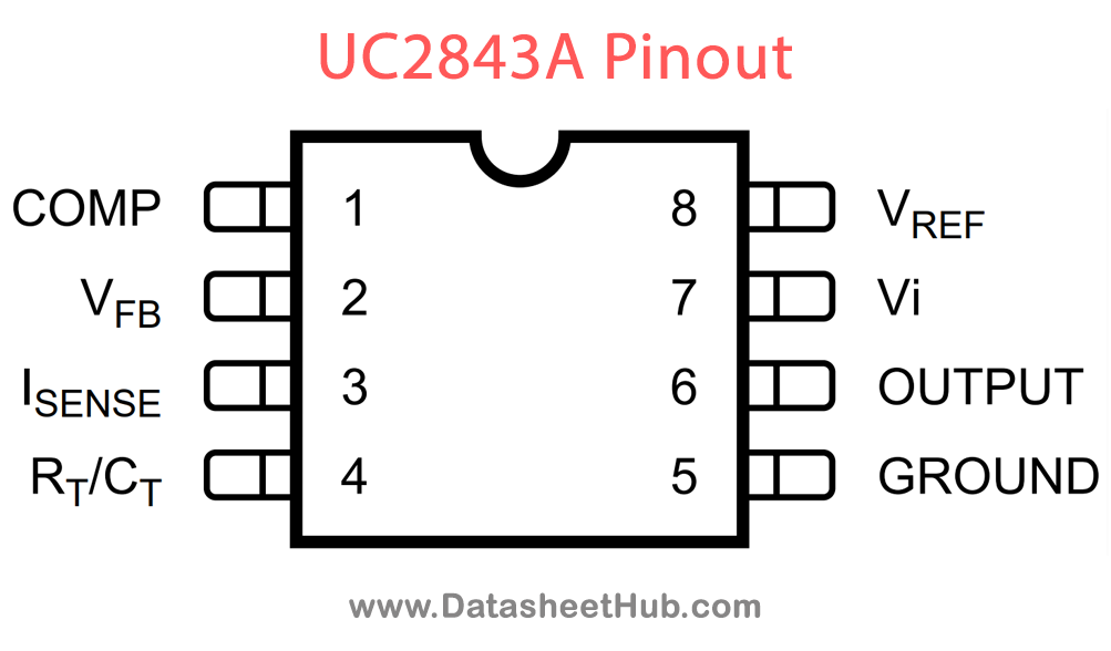
| Pin | Description |
|---|---|
| COMP | This pin is the Error Amplifier output and is made available for loop compensation. |
| VFB | This is the inverting input of the Error Amplifier. It is normally connected to the switching power supply output through a resistor divider. |
| ISENSE | A voltage proportional to inductor current is connected to this input. The PWM uses this information to terminate the output switch conduction. |
| RT/CT | The oscillator frequency and maximum Output duty cycle are programmed by connecting resistor RT to Vref and cpacitor CT to ground. Operation to 500kHz is possible. |
| GROUND | This pin is the combined control circuitry and power ground. |
| OUTPUT | This output directly drives the gate of a power MOSFET. Peak currents up to 1A are sourced and sunk by this pin. |
| VCC | This pin is the positive supply of the control IC. |
| Vref | This is the reference output. It provides charging current for capacitor CT through resistor RT. |
Absolute maximum ratings
| Parameter | Symbol | Value | Unit |
|---|---|---|---|
| Supply Voltage (low impedance source) | Vi | 30 | V |
| Supply Voltage (Ii < 30mA) | Vi | Self Limiting | |
| Output Current | IO | ±1 | A |
| Output Energy (capacitive load) | EO | 5 | mJ |
| Analog Inputs (pins 2, 3) | – 0.3 to 5.5 | V | |
| Error Amplifier Output Sink Current | 10 | mA | |
| Power Dissipation at Tamb £ 25 °C (DIP-8) | Ptot | 1.25 | W |
| Power Dissipation at Tamb £ 25 °C (SO-8) | Ptot | 800 | mW |
| Storage Temperature Range | Tstg | – 65 to 150 | °C |
| Junction Operating Temperature | TJ | – 40 to 150 | °C |
| Lead Temperature (soldering 10s) | TL | 300 | °C |
UC2843A applications
- Battery Chargers
- Power Management
- LED Drivers
- Inverters
Comments 0
Leave a comment