

74HC4066 Datasheet – Quadruple Bilateral Analog Switch
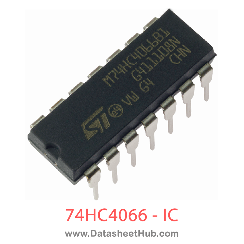
74HC4066 overview
The 74HC4066 is a Quadruple Bilateral Analog Switch made by Philips Electronics - NXP, supplied in these packages: SOIC, SSOP, TSSOP, PDIP type. The absolute maximum ratings table on this page lists the 9 limits from the manufacturer's datasheet that must not be exceeded. This page brings together the 74HC4066 pinout, key specifications and maximum ratings, with the full datasheet PDF to preview below or download.
The 74HC4066; 74HCT4066 is a quad single pole, single throw analog switch. Each switch features two input/output terminals (nY and nZ) and an active HIGH enable input (nE). When nE is LOW, the analog switch is turned off. Inputs include clamp diodes. This enables the use of current limiting resistors to interface inputs to voltages in excess of VCC.
Key specifications
Datasheet
74HC4066 features
- n Input levels nE inputs
- u For 74HC4066: CMOS level
- u For 74HCT4066: TTL level
- n Low ON resistance
- u 50 W (typical) at VCC = 4.5 V
- u 45 W (typical) at VCC = 6.0 V
- u 35 W (typical) at VCC = 9.0 V
- n Specified in compliance with JEDEC standard no. 7A
- n ESD protection
- u HBM JESD22-A114F exceeds 2000 V
- u MM JESD22-A115-A exceeds 200 V
- n Multiple package options
- n Specified from -40 °C to +85 °C and -40 °C to +125 °C
74HC4066 pinout
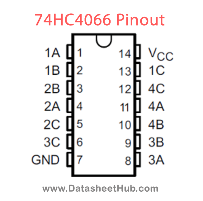
| Pin | Name | Description |
|---|---|---|
| 2, 3, 9, 10 | 1Z, 2Z, 3Z, 4Z | independent input or output |
| 1, 4, 8, 11 | 1Y, 2Y, 3Y, 4Y | independent input or output |
| 7 | GND | ground (0 V) |
| 13, 5, 6, 12 | 1E, 2E, 3E, 4E | enable input (active HIGH) |
| 14 | VCC | supply voltage |
Absolute maximum ratings
| Parameter | Symbol | Value | Unit | Conditions |
|---|---|---|---|---|
| supply voltage | VCC | Min -0.5 / Max +11.0 | V | |
| input clamping current | IIK | Max ±20 | mA | VI < -0.5 V or VI > VCC + 0.5 V |
| switch clamping current | ISK | Max ±20 | mA | VSW < -0.5 V or VSW > VCC + 0.5 V |
| switch current | ISW | Max ±25 | mA | VSW = -0.5 V to VCC + 0.5 V [1] |
| supply current | ICC | Max 50 | mA | |
| ground current | IGND | Max -50 | mA | |
| storage temperature | Tstg | Min -65 / Max +150 | °C | |
| - | SO14, (T) SSOP14 and DHVQFN14 packages | Min mW | 500 | |
| power dissipation | P | Max 100 | mW | per switch |
Comments 0
Leave a comment