

74LS74A Datasheet – Dual D-Type Edge-triggered Flip-Flop
DUAL D-TYPE POSITIVE-EDGE-TRIGGERED FLIP-FLOPS WITH PRESET AND CLEAR
Package DIP 14 Pin Type Series 74LS

74LS74A overview
The SN54 / 74LS74A dual edge-triggered flip-flop utilizes Schottky TTL circuitry to produce high speed D-type flip-flops. Each flip-flop has individual clear and set inputs, and also complementary Q and Q outputs.
Information at input D is transferred to the Q output on the positive-going edge of the clock pulse. Clock triggering occurs at a voltage level of the clock pulse and is not directly related to the transition time of the positive-going pulse. When the clock input is at either the HIGH or the LOW level, the D input signal has no effect.
Datasheet
74ls74a-datasheet.pdf
74LS74A features
- Dual Flip-Flops in One Package
- Positive-Edge Triggered
- Clear and Preset Inputs
- Wide Operating Voltage Range
- TTL Logic Compatibility
- Low Power Consumption
- High-Speed Operation
- Data Retention on Power Loss
- Compact DIP Package
- Versatile for Sequential Logic
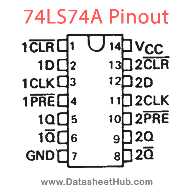
74LS74A pinout
74LS74A applications
- Flip-Flop Circuit
- Sequential Logic Design
- Clock Division and Synchronization
- Frequency Division
Comments 0
Leave a comment