
89V52RD2 Datasheet – FlashFlex51, 8-bit Microcontroller
FlashFlex51 MCU, 8-bit Microcontroller
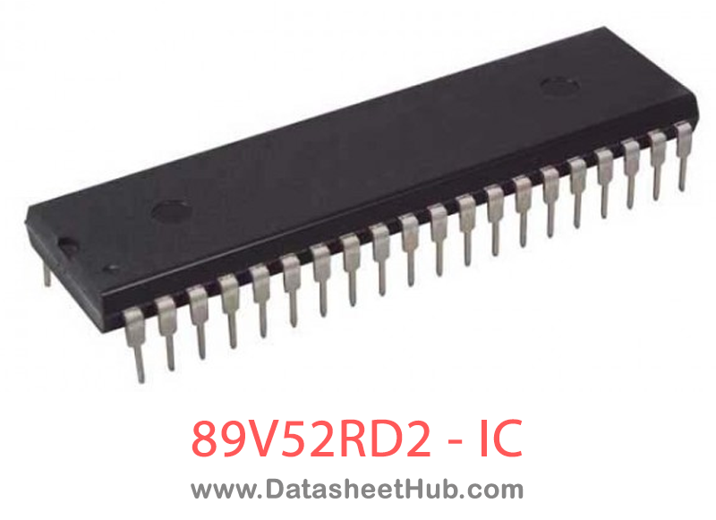
89V52RD2 overview
The 89V52RD2 is a FlashFlex51 MCU, 8-bit Microcontroller made by Silicon Storage Technology, supplied in these packages: 40-pin PDIP, 44-lead PLCC, 44-lead TQFP. The absolute maximum ratings table on this page lists the 8 limits from the manufacturer's datasheet that must not be exceeded. This page brings together the 89V52RD2 pinout and maximum ratings, with the full datasheet PDF to preview below or download.
The SST89E5xxRD2 and SST89V5xxRD2 are members of the FlashFlex51 family of 8-bit microcontroller products designed and manufactured with SST’s patented and proprietary Super Flash CMOS semiconductor process technology. The split-gate cell design and thick-oxide tunneling injector offer significant cost and reliability benefits for SST’s customers. The devices use the 8051 instruction set and are pin-for-pin compatible with standard 8051 microcontroller devices.
The devices come with 16/24/40/72 KByte of on-chip flash EEPROM program memory which is partitioned into 2 independent program memory blocks. The primary Block 0 occupies 8/16/32/64 KByte of internal program memory space and the secondary Block 1 occupies 8 KByte of internal program memory space.
The 8-KByte secondary block can be mapped to the lowest location of the 8/16/32/64 KByte address space; it can also be hidden from the program counter and used as an independent EEPROM-like data memory.
In addition to the 16/24/40/72 KByte of EEPROM program memory on-chip, the devices can address up to 64 KByte of external program memory. In addition to 1024 x8 bits of on-chip RAM, up to 64 KByte of external RAM can be addressed. The flash memory blocks can be programmed via a standard 87C5x OTP EPROM programmer fitted with a special adapter and the firmware for SST’s devices. During power- on reset, the devices can be configured as either a slave to an external host for source code storage or a master to an external host for an in-application programming (IAP) operation. The devices are designed to be programmed in-system and in-application on the printed circuit board for maximum flexibility. The devices are pre-programmed with an example of the bootstrap loader in the memory, demonstrating the initial user program code loading or subsequent user code updating via the IAP operation. The sample bootstrap loader is available for the user’s reference and convenience only; SST does not guarantee its functionality or usefulness. Chip-Erase or Block-Erase operations will erase the pre-programmed sample code
89V52RD2 features
- Fully Software Compatible
- Development Toolset Compatible
- Pin-For-Pin Package Compatible
- SST89E5xxRD2 Operation 0 to 40 MHz at 5V
- 0 to 40 MHz at 5V
- SST89V5xxRD2 Operation
- 0 to 33 MHz at 3V
- 1 KByte Internal RAM
- Dual Block Super Flash EEPROM
- 8/16/32/64 KByte primary block + 8 KByte secondary block
- Memory Overlay for Interrupt Support during IAP (128-Byte sector size for both blocks)
- Individual Block Security Lock with Soft Lock
- Concurrent Operation during In-Application Programming (IAP)
- Support External Address Range up to 64 KByte of Program and Data Memory
- Three High-Current Drive Ports (16 mA each)
- Three 16-bit Timers/Counters
- Full-Duplex, Enhanced UARTFraming Error Detection Automatic Address Recognition
- Framing Error Detection
- Automatic Address Recognition
- Ten Interrupt Sources at 4 Priority Levels Four External Interrupt Inputs
- Four External Interrupt Inputs
- Programmable Watchdog Timer (WDT)
- Programmable Counter Array (PCA)
- Four 8-bit I/O Ports (32 I/O Pins) and One 4-bit Port
- Second DPTR register
- Low EMI Mode (Inhibit ALE)
- SPI Serial Interface
- Standard 12 Clocks per cycle, the device has an option to double the speed to 6 clocks per cycle.
- TTL- and CMOS-Compatible Logic Levels
- Brown-out Detection
- Low Power Modes Power-down Mode with External Interrupt Wake-up Idle Mode
- Power-down Mode with External Interrupt Wake-up
- Idle Mode
- Temperature Ranges: Commercial (0°C to +70°C) Industrial (-40°C to +85°C)
- Commercial (0°C to +70°C)
- Industrial (-40°C to +85°C)
- Packages Available 44-lead PLCC 40-pin PDIP (Port 4 feature not available) 44-lead TQFP
- 44-lead PLCC
- 40-pin PDIP (Port 4 feature not available)
89V52RD2 pinout
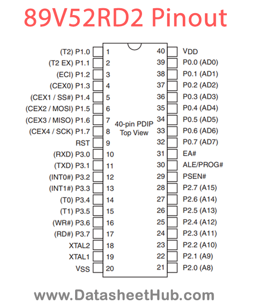
| Name | Description |
|---|---|
| P0[7:0] | Port 0: Port 0 is an 8-bit open drain bi-directional I/O port. As an output port each pin can sink several LS TTL inputs. Port 0 pins float that have ‘1’s written to them, and in this state can be used as high-impedance inputs. Port 0 is also the multiplexed low-order address and data bus during acc |
| P1[7:0] | Port 1: Port 1 is an 8-bit bi-directional I/O port with internal pull-ups. The Port 1 output buff- ers can drive LS TTL inputs. Port 1 pins are pulled high by the internal pull-ups when “1”s are written to them and can be used as inputs in this state. As inputs, Port 1 pins that are externally pulle |
| P1[0] | T2: External count input to Timer/Counter 2 or Clock-out from Timer/Counter 2 |
| P1[1] | T2EX: Timer/Counter 2 capture/reload trigger and direction control |
| P1[2] | ECI: PCA Timer/Counter External Input: This signal is the external clock input for the PCA timer/counter. |
| P1[3] | CEX0: Compare/Capture Module External I/O Each compare/capture module connects to a Port 1 pin for external I/O. When not used by the PCA, this pin can handle standard I/O. |
| P1[4] | SS#: Master Input or Slave Output for SPI. OR CEX1: Compare/Capture Module External I/O |
| P1[5] | MOSI: Master Output line, Slave Input line for SPI OR CEX2: Compare/Capture Module External I/O |
| P1[6] | MISO: Master Input line, Slave Output line for SPI OR CEX3: Compare/Capture Module External I/O |
| P1[7] | SCK: Master clock output, slave clock input line for SPI OR CEX4: Compare/Capture Module External I/O |
| P2[7:0] | Port 2: Port 2 is an 8-bit bi-directional I/O port with internal pull-ups. Port 2 pins are pulled high by the internal pull-ups when “1”s are written to them and can be used as inputs in this state. As inputs, Port 2 pins that are externally pulled low will source current because of the internal pul |
| P3[7:0] | Port 3: Port 3 is an 8-bit bidirectional I/O port with internal pull-ups. The Port 3 output buff- ers can drive LS TTL inputs. Port 3 pins are pulled high by the internal pull-ups when “1”s are written to them and can be used as inputs in this state. As inputs, Port 3 pins that are externally pulled |
| P3[0] | RXD: Universal Asynchronous Receiver/Transmitter (UART) - Receive input |
| P3[1] | TXD: UART - Transmit output |
| P3[2] | INT0#: External Interrupt 0 Input |
Absolute maximum ratings
| Parameter | Value |
|---|---|
| Ambient Temperature Under Bias | -55°C to +125°C |
| Storage Temperature | -65°C to +150°C |
| Maximum IOL per I/O Pins P1.5, P1.6, P1.7 | 20mA |
| Maximum IOL per I/O for All Other Pins | 15mA |
| Package Power Dissipation Capability (Ta = 25°C) | 1.5W |
| Through Hole Lead Soldering Temperature (10 Seconds) | 300°C |
| Surface Mount Lead Soldering Temperature (3 Seconds) | 240°C |
| Output Short Circuit Current1 | 50mA |
89V52RD2 applications
- Microcontroller-based Systems
- Embedded Control Applications
- Industrial Automation
- Robotics Control
Comments 0
Leave a comment