

AM28F020A Datasheet – 2 Megabit Flash Memory – AMD
2 Megabit (256 K x 8-Bit) CMOS 12.0 Volt, Bulk Erase Flash Memory
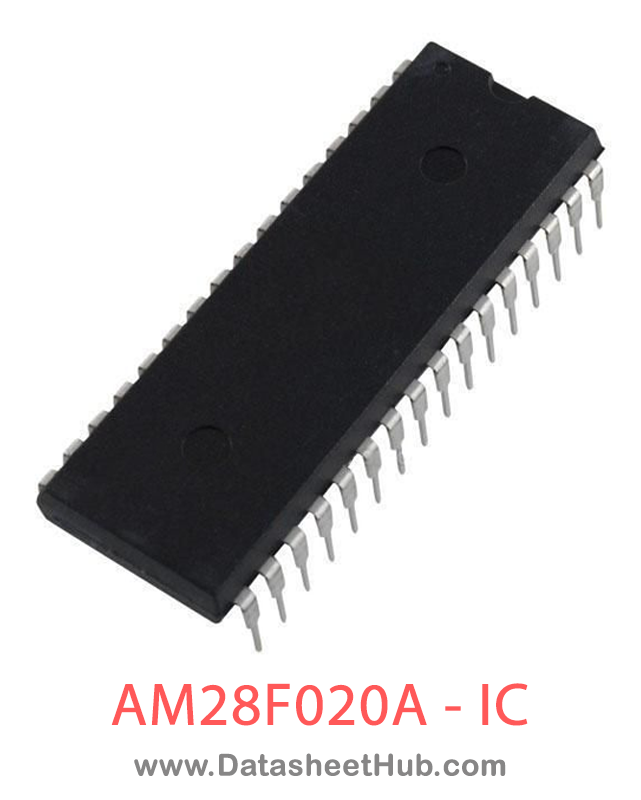
AM28F020A overview
The AM28F020A is a 2 Megabit (256 K x 8-Bit) CMOS 12.0 Volt, Bulk Erase Flash Memory made by Advanced Micro Devices, supplied in these packages: DIP, PLCC, TSOP 32 Pin Type. The absolute maximum ratings table on this page lists the 4 limits from the manufacturer's datasheet that must not be exceeded. This page brings together the AM28F020A pinout and maximum ratings, with the full datasheet PDF to preview below or download.
The Am28F020A is a 2 Megabit Flash memory organized as 256 Kbytes of 8 bits each. AMD’s Flash memories offer the most cost-effective and reliable read/ write non-volatile random access memory. The Am28F020A is packaged in 32-pin PDIP, PLCC, and TSOP versions. It is designed to be reprogrammed and erased in-system or in standard EPROM programmers. The Am28F020A is erased when shipped from the factory.
The standard Am28F020A offers access times of as fast as 70 ns, allowing high speed microprocessors to operate without wait states. To eliminate bus contention, the device has separate chip enable (CE#) and output enable (OE#) controls.
AMD’s Flash memories augment EPROM functionality with in-circuit electrical erasure and programming. The Am28F020A uses a command register to manage this functionality. The command register allows for 100% TTL level control inputs and fixed power supply levels during erase and programming, while maintaining maximum EPROM compatibility.
The Am 28 F020A is compatible with the AMD Am28F256A, Am28F512A, and Am28F010A Flash memories. All devices in the Am28Fxxx family follow the JEDEC 32-pin pinout standard. In addition, all devices within this family that offer Embedded Algorithms use the same command set. This offers designers the flexibility to retain the same device foot- print and command set, at any density between 256 Kbits and 2 Mbits.
AMD’s Flash technology reliably stores memory con- tents even after 100,000 erase and program cycles. The AMD cell is designed to optimize the erase and programming mechanisms. In addition, the combination of advanced tunnel oxide processing and low internal electric fields for erase and programming operations produces reliable cycling. The Am28F020A uses a 12.0±5% VPP supply input to perform the erase and programming functions.
The highest degree of latch-up protection is achieved with AMD’s proprietary non-epi process. Latch-up protection is provided for stresses up to 100 mA on address and data pins from –1 V to VCC +1 V.
AMD’s Flash technology combines years of EPROM and EEPROM experience to produce the highest levels of quality, reliability, and cost effectiveness. The Am28F020A electrically erases all bits simultaneously using Fowler-Nordheim tunneling. The bytes are programmed one byte at a time using the EPROM programming mechanism of hot electron injection.
Datasheet
AM28F020A features
- High performance Access times as fast as 70 ns
- Access times as fast as 70 ns
- CMOS low power consumption
- 30 mA maximum active current
- 100 µA maximum standby current
- No data retention power consumption
- Compatible with JEDEC-standard byte-wide 32-pin EPROM pinouts 32-pin PDIP 32-pin PLCC 32-pin TSOP
- 32-pin PDIP
- 32-pin PLCC
- 32-pin TSOP
- 100,000 write/erase cycles minimum
- Write and erase voltage 12.0 V ±5%
- Latch-up protected to 100 mA from –1 V to VCC +1 V
- –1 V to VCC +1 V
- Embedded Erase Electrical Bulk Chip Erase Five seconds typical chip erase, including pre-programming
- Five seconds typical chip erase, including pre-programming
- Embedded Program
- 14 µs typical byte program, including time-out
- 4 seconds typical chip program
- Command register architecture for microprocessor/microcontroller compatible write interface
- On-chip address and data latches
- Advanced CMOS flash memory technology Low cost single transistor memory cell
- Low cost single transistor memory cell
- Embedded algorithms for completely self-timed write/erase operations
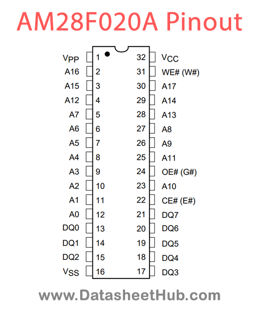
AM28F020A pinout
| Name | Description |
|---|---|
| A0-A17 | Address Inputs for memory locations. Internal latches hold addresses during write cycles. |
| CE#(E#) | Chip Enable active low input activates the chip’s control logic and input buffers. Chip Enable high will deselect the device and operates the chip in stand-by mode. |
| DQ0-DQ7 | Data Inputs during memory write cycles. Internal latches hold data during write cycles. Data Outputs during memory read cycles. |
| NC | No Connect-corresponding pin is not connected inter- nally to the die. |
| OE#(G#) | Output Enable active low input gates the outputs of the device through the data buffers during memory read cycles. Output Enable is high during command sequencing and program/erase operations. |
| VPP | Program voltage input. VPP must be at high voltage in order to write to the command register. The command register controls all functions required to alter the memory array contents. Memory contents cannot be altered when VPP £ VCC +2 V. |
| VCC | Power supply for device operation. (5.0 V ± 5% or 10%) |
| VSS | Ground |
| WE#(W#) | Write Enable active low input controls the write function of the command register to the memory array. The tar- get address is latched on the falling edge of the Write Enable pulse and the appropriate data is latched on the rising edge of the pulse. Write Enable high inhibits writ- ing to the device |
Absolute maximum ratings
| Parameter | Value |
|---|---|
| Storage Temperature | 65°C to +125°C |
| Ambient Temperaturewith Power Applied | 55°C to +125°C |
| Voltage with Respect to Ground All pins except A9 and VPP (Note 1) | .–2.0 V to +7.0 V |
| Output Short Circuit Current (Note 3) | 200 mA |
Comments 0
Leave a comment