

BQ24721 Datasheet – Switch-Mode Charger IC
Adv Multi-Chemistry Multi-Cell Sync Switch-Mode Charger Syst Power Selector (Rev. F)
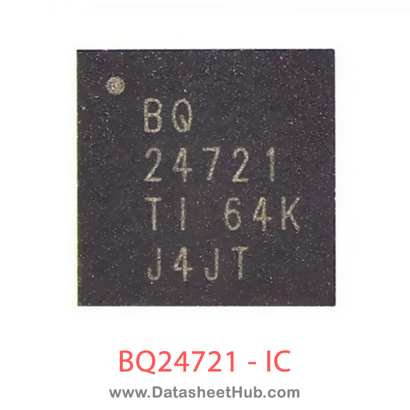
BQ24721 overview
The BQ24721 is an Adv Multi-Chemistry Multi-Cell Sync Switch-Mode Charger Syst Power Selector (Rev. F) made by Texas Instruments, supplied in a VQFN 32 Pin Type package. The absolute maximum ratings table on this page lists the 3 limits from the manufacturer's datasheet that must not be exceeded. This page brings together the BQ24721 pinout and maximum ratings, with the full datasheet PDF to preview below or download.
The bq24721 is a high efficiency synchronous battery pack charger with high level of integration for portable applications. This device implements a high performance analog front-end that interfaces to the system power management micro-controller through a simplified SBS-like SMBus interface.
The dynamic power management (DPM) function modifies the charge current depending on system load conditions, avoiding ac adapter overload.
High accuracy current sense amplifiers enable accurate measurement of either the charge current or the ac adapter current, allowing termination of non smart packs and monitoring of overall system power.
The adapter isolation diode can be bypassed or entirely replaced with an external MOSFET using a control signal provided by the bq24721, thus reducing overall power dissipation.
Integrated features such as charger soft start, charge overcurrent protection, and IC temperature monitoring provide a second level of protection, in addition to pack and system protection functions.
Datasheet
BQ24721 features
- High Efficiency NMOS-NMOS Synchronous Buck Converter With User-Selectable 300 kHz Portable DVD Players or 500 kHz frequency
- bq24721C Offers Softer Turn-On, Stronger Turn off
- SBS-Like (1) SMBus Interface for Control and Status Communications With Host
- Programmable Battery Voltage, Charge Current, and AC Adapter Current via SBS-Like SMBus Interface
- 0.4% Charge Voltage Regulation Accuracy
- 3% Charge Current Regulation Accuracy
- 3% Adapter Current Regulation Accuracy Dynamic Power Management (DPM)
- 2% Accuracy Integrated Charge and AC Adapter 20× Current Amplifier Output
- 3-Cell and 4-Cell Li-Ion Voltage Regulation 9 V, 12 V–14.4 V, 16 V–19.2 V
- Battery Pack Voltage Operating Range 0 V–19.2 V
- AC Adapter Operating Range 8 V–28 V
- 99.5% Max Duty Cycle
- Internal Soft Start
- Integrated 5% 5-V LDO When AC Adapter Applied
- 6-V Drive Supply Voltage for Increased Efficiency
- Reverse Battery to Adapter Discharge Protection
- Battery/Adapter to System Power Selector Function
- Charge and Adapter Overcurrent Protection
- Battery Thermistor Sense, TS, Comparators
- Available in 32-Pin 5x5-mm QFN Package
BQ24721 pinout
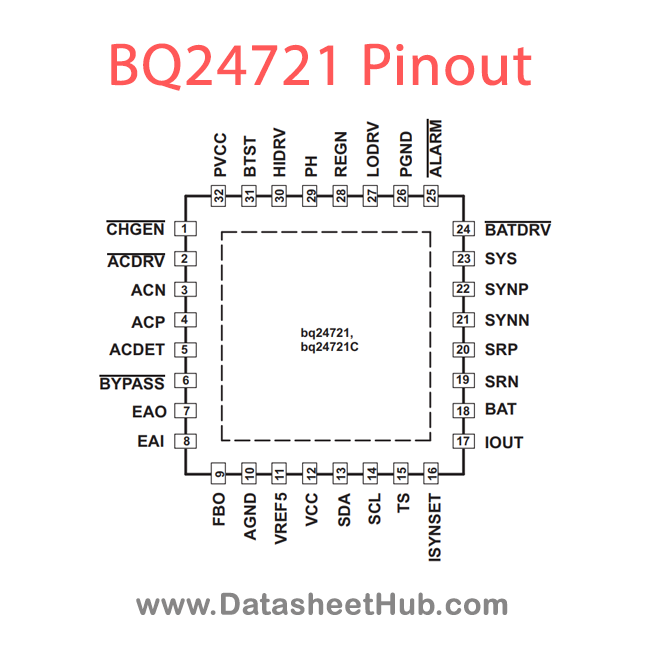
| Pin | Name | Description |
|---|---|---|
| 1 | CHGEN | Charge enable logic level low input. Logic HI on the CHGEN pin disables the charger. Logic LO on the CHGEN pin enables the charger. When the SMBus control register = bit0, CHGEN is also LO. |
| 2 | ACDRV | AC adapter to system switch driver output. Connect directly to the gate of the ACFET PMOS power FET. Connect the FET source to the PVCC node and negative side of the input current-sense resistor. Connect the FET drain to the system load side. Recommend placing a 100-kΩ resistor from the gate to the |
| 3 | ACN | Adapter current sense resistor, negative input. An optional 0.1-mF ceramic capacitor is placed from this pin to AGND for common-mode filtering. An optional 0.1-mF ceramic capacitor is placed from ACN to ACP to provide differential-mode filtering. |
| 4 | ACP | Adapter current sense resistor, positive input. Place this on the adapter side of the input current sense resistor. Recommend placing a 0.1-mF ceramic capacitor from ACP to AGND to provide common-mode filtering. |
| 5 | ACDET | AC adapter detected sense voltage input. Connect a voltage divider resistor from adapter input (before Bypass FET) to ACDET, and another resistor from ACDET to AGND, in order to program adapter detect threshold of 1.2 V. ACDET threshold should be greater than maximum battery regulation voltage, and |
| 6 | BYPASS | Gate drive for the adapter input BYPASS switch to prevent reverse discharge from the battery to the input. Connect this pin directly to the gate of the input bypass PMOS power FET. The source of the FET is connected to the adapter input voltage node. Recommend placing a 10-kΩ resistor from the gate |
| 7 | EAO | Error amplifier output for compensation. Connect the feedback compensation components from EAO to EAI. Typically a capacitor in parallel with a series resistor and capacitor. See the compensation calculation procedures. This node is internally compared to the PWM saw-tooth oscillator. |
Absolute maximum ratings
| Parameter | Value |
|---|---|
| Operating ambient temperature range (TA) | Value / unit –40°C to 85°C |
| Maximum junction temperature (TJ_MAX) | Value / unit 150°C |
| Storage temperature range (Tstg) | Value / unit –65°C to 150°C |
BQ24721 applications
- Portable Notebook Computers
- Portable DVD Players
- Webpads, PC Tablets
Comments 0
Leave a comment