

BS003F3P6 Datasheet – 8S003F3P6, 8-bit Microcontroller
8-bit Microcontrollers – MCU 8-bit MCU Value Line 16 MHz 8kb FL 128EE
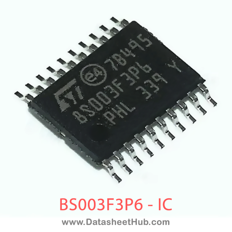
BS003F3P6 overview
The BS003F3P6 is an 8-bit Microcontrollers – MCU 8-bit MCU Value Line 16 MHz 8kb FL 128EE made by STMicroelectronics, supplied in a TSSOP 20 Pin Type package. The absolute maximum ratings table on this page lists the 5 limits from the manufacturer's datasheet that must not be exceeded. This page brings together the BS003F3P6 pinout and maximum ratings, with the full datasheet PDF to preview below or download.
The STM8S003F3/K3 value line 8-bit microcontrollers offer 8 Kbytes of Flash program memory, plus integrated true data EEPROM. They are referred to as low-density devices in the STM8S microcontroller family reference manual (RM0016).
The STM8S003F3/K3 value line devices provide the following benefits: performance, robustness and reduced system cost.
Device performance and robustness are ensured by true data EEPROM supporting up to 100000 write/erase cycles, advanced core and peripherals made in a state-of-the-art technology at 16 MHz clock frequency, robust I/Os, independent watchdogs with separate clock source, and a clock security system.
The system cost is reduced thanks to a high system integration level with internal clock oscillators, watchdog, and brown-out reset. Full documentation is offered as well as a wide choice of development tools.
Datasheet
BS003F3P6 features
- Core
- 16 MHz advanced STM8 core with Harvard architecture and 3-stage pipeline
- Extended instruction set
- Memories
- Program memory: 8 Kbyte Flash memory; data retention 20 years at 55 °C after 100 cycles
- RAM: 1 Kbyte
- Data memory: 128 bytes true data EEPROM; endurance up to 100 k write/erase cycles
- Clock, reset and supply management
- 2.95 V to 5.5 V operating voltage
- Flexible clock control, 4 master clock sources
- Low-power crystal resonator oscillator
- External clock input
- Internal, user-trimmable 16 MHz RC
- Internal low-power 128 kHz RC
- Clock security system with clock monitor
- Power management
- Low-power modes (wait, active-halt, halt)
- Switch-off peripheral clocks individually
- Permanently active, low-consumption power-on and power-down reset
- Interrupt management
- Nested interrupt controller with 32 interrupts
- Up to 27 external interrupts on 6 vectors
- Timers
- Advanced control timer: 16-bit, 4 CAPCOM channels, 3 complementary outputs, dead-time insertion and flexible synchronization
- 16-bit general purpose timer, with 3 CAPCOM channels (IC, OC or PWM)
- 8-bit basic timer with 8-bit prescaler
- Auto wakeup timer
- Window and independent watchdog timers
- Communications interfaces
- UART with clock output for synchronous operation, Smart Card, IrDA, LIN master mode
- SPI interface up to 8 Mbit/s
- I2C interface up to 400 Kbit/s
- Analog to digital converter (ADC) 10-bit ADC, ± 1 LSB ADC with up to 5 multiplexed channels, scan mode and analog watchdog
- 10-bit ADC, ± 1 LSB ADC with up to 5 multiplexed channels, scan mode and analog watchdog
- I/Os
- Up to 28 I/Os on a 32-pin package including 21 high-sink outputs
- Highly robust I/O design, immune against current injection
- Development support Embedded single-wire interface module (SWIM) for fast on-chip programming and non- intrusive debugging
- Embedded single-wire interface module (SWIM) for fast on-chip programming and non- intrusive debugging
BS003F3P6 pinout
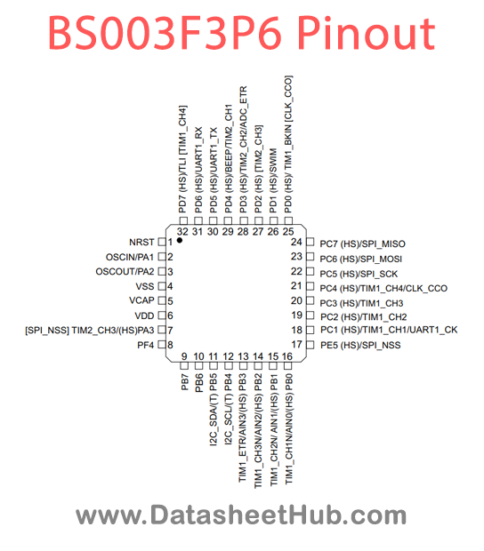
| Name | Description |
|---|---|
| wpu | OD |
| PA2/OSCOUT | X |
| VSS | - |
| VCAP | - |
| VDD | - |
| PA3/TIM2_CH3 [SPI_NSS] | X |
| PF4 | - |
| PB7 | - |
| PB6 | - |
| PB5/I2C_SDA | X |
| PB4/I2C_SCL | X |
| PB3/AIN3 [TIM1_ETR] | X |
| PB2/AIN2 [TIM1_CH3N] | X |
| PB1/AIN1 [TIM1_CH2N] | X |
| PB0/AIN0 [TIM1_CH1N] | X |
| PE5/SPI_NSS | X |
| PC1/TIM1_CH1/ UART1_CK | X |
| PC2/TIM1_CH2 | X |
| PC3/TIM1_CH3 | X |
Absolute maximum ratings
| Parameter | Symbol | Value | Unit |
|---|---|---|---|
| Supply voltage (1) | VDDx - VSS | Min -0.3 / Max 6.5 | V |
| Input voltage on true open drain pins (2) | VIN | Min VSS - 0.3 / Max 6.5 | |
| VSS - 0.3 | Input voltage on any other pin (2) | Min VDD + 0.3 | |
| Variations between different power pins | |VDDx - VDD| | Max 50 | mV |
| Variations between all the different ground pins | |VSSx - VSS| | Max 50 |
Comments 0
Leave a comment