

F9444ZZ Datasheet – 8-bit Microcontroller – Fujitsu, Samsung
Integrated Circuit
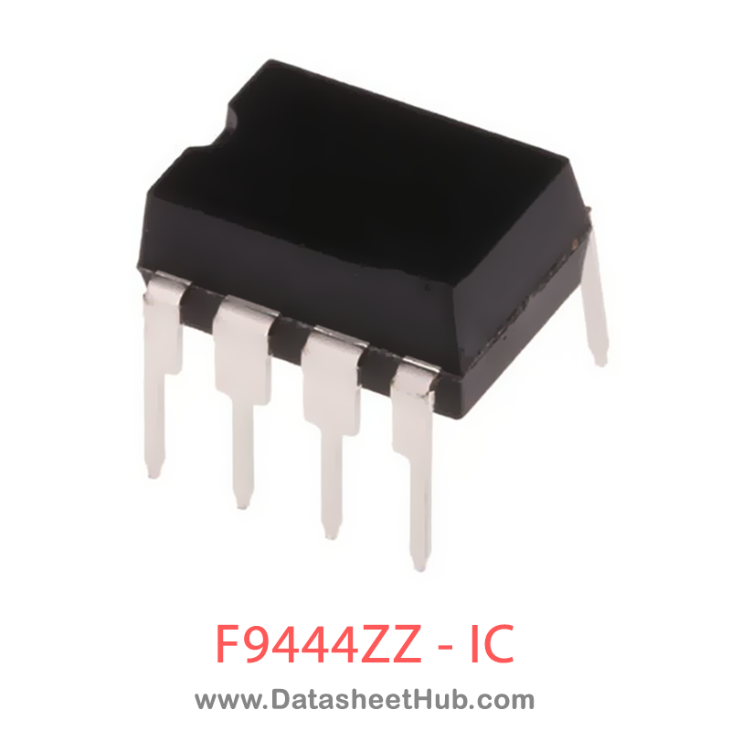
F9444ZZ overview
The F9444ZZ is an Integrated Circuit made by Fairchild Semiconductor, supplied in a DIP 8 Pin Type package. The absolute maximum ratings table on this page lists the 7 limits from the manufacturer's datasheet that must not be exceeded. This page brings together the F9444ZZ pinout and maximum ratings, with the full datasheet PDF to preview below or download.
The S3C9442/C9444/C9452/C9454 single-chip 8-bit microcontroller is designed for useful A/D converter , SIO application field. The S3C9442/C9444/C9452/C9454 uses powerful SAM88RCRI CPU and S3C9442/C9444/C9452/C9454 architecture. The internal register file is logically expanded to increase the on- chip register space.
The S3C9442/C9444/C9452/C9454 has 2K/4K bytes of on-chip program ROM and 208 bytes of RAM. The S3C9442/C9444/C9452/C9454 is a versatile general-purpose microcontroller that is ideal for use in a wide range of electronics applications requiring simple timer/counter, PWM. In addition, the S3C9442/C9444/C9452/C9454’s advanced CMOS technology provides for low power consumption and wide operating voltage range.
Using the SAM88RCRI design approach, the following peripherals were integrated with the SAM88RCRI core:
The S3C9442/C9444/C9452/C9454 microcontroller is ideal for use in a wide range of electronic applications requiring simple timer/counter, PWM, ADC. S3C9452/C9454 is available in a 20/16-pin DIP and a 20-pin SOP package. S3C9452/C9454 is available in a 8-pin and a 8-pin SOP package.
Datasheet
F9444ZZ features
- CPU SAM88RCRI CPU core The SAM88RCRI core is low-end version of the current SAM87 core.
- SAM88RCRI CPU core
- The SAM88RCRI core is low-end version of the current SAM87 core.
- Memory 2/4-Kbyte internal program memory 208-byte general purpose register area
- 2/4-Kbyte internal program memory
- 208-byte general purpose register area
- Instruction Set
- 41 instructions
- The SAM88RCRI core provides all the SAM87 core instruction except the word-oriented instruction, multiplication, division, and some one-byte instruction.
- Instruction Execution Time 400 ns at 10 MHz fOSC (minimum)
- 400 ns at 10 MHz fOSC (minimum)
- Interrupts 4 interrupt sources with one vector One interrupt level
- 4 interrupt sources with one vector
- One interrupt level
- General I/O Three I/O ports (Max 18 pins) Bit programmable ports
- Three I/O ports (Max 18 pins)
- Bit programmable ports
- 8-bit High-speed PWM 8-bit PWM 1-ch (Max: 156 kHz) 6-bit base + 2-bit extension
- 8-bit PWM 1-ch (Max: 156 kHz)
- 6-bit base + 2-bit extension
- Built-in reset Circuit Low voltage detector for safe reset
- Low voltage detector for safe reset
- Timer/Counters
- One 8-bit basic timer for watchdog function
- One 8-bit timer/counter with time interval modes
- A/D Converter Nine analog input pins 10-bit conversion resolution
- Nine analog input pins
- 10-bit conversion resolution
- Oscillation Frequency
- 1 MHz to 10 MHz external crystal oscillator
- Maximum 10 MHz CPU clock
- Internal RC: 3.2 MHz (typ.), 0.5 MHz (typ.) in VDD = 5 V
- Operating Temperature Range – 40°C to + 85°C
- – 40°C to + 85°C
- Operating Voltage Range 2.0 V (LVR Level) to 5.5 V
- 2.0 V (LVR Level) to 5.5 V
- Smart Option
- Package Types S3C9452/C9454: 20-DIP-300A 20-SOP-375 16-DIP-300A S3C9442/C9444 8-DIP-300 8-SOP-225
- S3C9452/C9454: 20-DIP-300A 20-SOP-375 16-DIP-300A
- 20-DIP-300A
F9444ZZ pinout
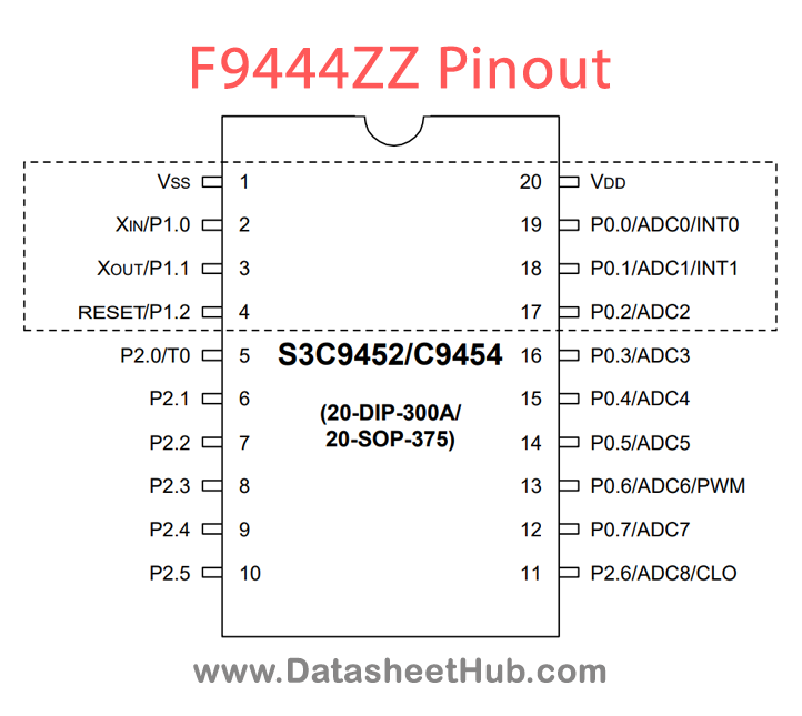
| Name | Description |
|---|---|
| P0.0–P0.7 | Bit-programmable I/O port for Schmitt trigger input or push-pull output. Pull-up resistors are assignable by software. Port0 pins can also be used as A/D converter input, PWM output or external interrupt input. |
| P1.0–P1.1 | Bit-programmable I/O port for Schmitt trigger input or push-pull, open-drain output. Pull-up resistors or pull-down resistors are assignable by software. |
| P1.2 | Schmitt trigger input port |
| P2.0–P2.6 | Bit-programmable I/O port for Schmitt trigger input or push-pull, open-drain output. Pull-up resistors are assignable by software. |
| XIN, XOUT | Crystal/Ceramic, or RC oscillator signal for system clock. |
| RESET | Internal LVR or External RESET |
| VDD, VSS | Voltage input pin and ground |
| CLO | System clock output port |
| INT0–INT1 | External interrupt input port |
| PWM | 8-Bit high speed PWM output |
| T0 | Timer0 match output |
| ADC0–ADC8 | A/D converter input |
Absolute maximum ratings
| Parameter | Symbol | Value | Unit | Conditions |
|---|---|---|---|---|
| Supply voltage | VDD | – 0.3 to + 6.5 | V | – |
| Input voltage | VI | – 0.3 to VDD + 0.3 | V | All ports |
| Output voltage | VO | – 0.3 to VDD + 0.3 | V | All output ports |
| Output current high | IOH | – 25 | mA | One I/O pin active |
| Output current low | IOL | + 30 | mA | One I/O pin active |
| Operating temperature | TA | – 40 to + 85 | °C | – |
| Storage temperature | TSTG | – 65 to + 150 | °C | – |
F9444ZZ applications
- Audio Amplifiers
- Sound Processing Systems
- Consumer Electronics
- Home Theater Systems
- Music Equipment
Comments 0
Leave a comment