
FP6321 Datasheet – Buck PWM DC-DC Controller
Synchronous Buck PWM DC-DC Controller
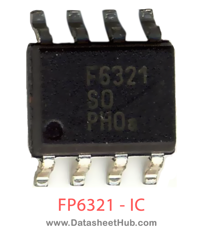
FP6321 overview
The FP6321 is a Synchronous Buck PWM DC-DC Controller, supplied in an SOP 8 Pin type package. The absolute maximum ratings table on this page lists the 13 limits from the manufacturer's datasheet that must not be exceeded. This page brings together the FP6321 pinout and maximum ratings, with the full datasheet PDF to preview below or download.
The FP6321 is designed to drive two N-channel MOSFETs in a synchronous rectified buck topology. It provides the output adjustment, internal soft-start, frequency compensation networks, monitoring and protection functions into a single package.
The IC operating at fixed 300kHz frequency provides simple, single feedback loop, voltage mode control with fast transient response. The resulting PWM duty ratio ranges from 0-100%.
The FP6321 features over current protection. The output current is monitored by sensing the voltage drop across the RDS-ON of the low side MOSFET which eliminates the need for a current sensing resistor. This device is available in SOP-8 package.
Datasheet
FP6321 features
- Operates from +5V or +12V
- Drives Two Low Cost N-Channel MOSFETs
- Fast Transient Response
- Simple Single-Loop Control Design ( Voltage-Mode PWM Control)
- Internal Soft-Start
- Over-Current Fault Monitor
- SOP-8 Package
- RoHS Compliant
FP6321 pinout
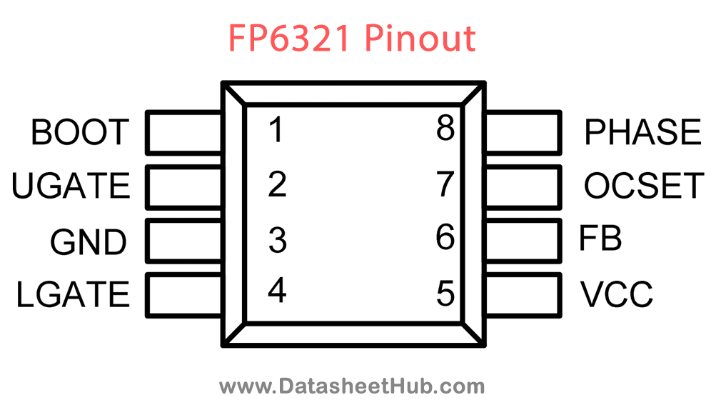
| Name | Description |
|---|---|
| BOOT | This pin provides bias voltage to the high side MOSFET Driver. A bootstrap circuit may be to create a BOOT voltage suitable to drive a standard N-Channel MOSFET. |
| UGATE | Connect UGATE to the high side MOSFET gate. This pin is monitored by the adaptive shoot-through protection circuitry to determine when the high side MOSFET has turned off. |
| GND | Ground. |
| LGATE | Connect LGATE to the low side MOSFET gate. This pin is monitored by the adaptive shoot-through protection circuitry to determine when the high side MOSFET has turned off. |
| VCC | Power Pin. |
| FB | Feedback Pin. The typical reference voltage is 0.8V. |
| OCSET | Shutdown Control and connect a resistance (ROCSET) for over current setting. |
| PHASE | Connect the PHASE pin to the high side MOSFET source, and sensing converter’s input power. |
Absolute maximum ratings
| Parameter | Value |
|---|---|
| VCC to GND | - 0.3V to +16V |
| BOOT, VBOOT-VPHASE | - 0.3V to +16V |
| PHASE | - 5V to +16V |
| UGATE | VPHASE - 0.3V to VBOOT +0.3V |
| LGATE | - 0.3V to VCC+0.3V |
| FB,OCSET to GND | - 0.3V to +6V |
| Power Dissipation @ TA=25℃, SOP-8 (PD) | 630mW |
| Package Thermal Resistance, SOP-8 (θJA) | 160°C/W |
| Junction Temperature | +150°C |
| Operation Temperature Range | 40°C to +85°C |
| Storage Temperature Range | 65°C to +150°C |
| Lead Temperature (Soldering, 10sec.) | +260°C |
| ESD Susceptibility HBM (Human Body Mode) MM (Machine Mode) | 2KV200V |
FP6321 applications
- Motherboard
- Graphic Card
- Telecomm Equipments
- High Power DC-DC Regulators
- Servers
Comments 0
Leave a comment