

HEF4053BT Datasheet – Multiplexer / Demultiplexer IC
Triple 2-channel analogue multiplexer/demultiplexer
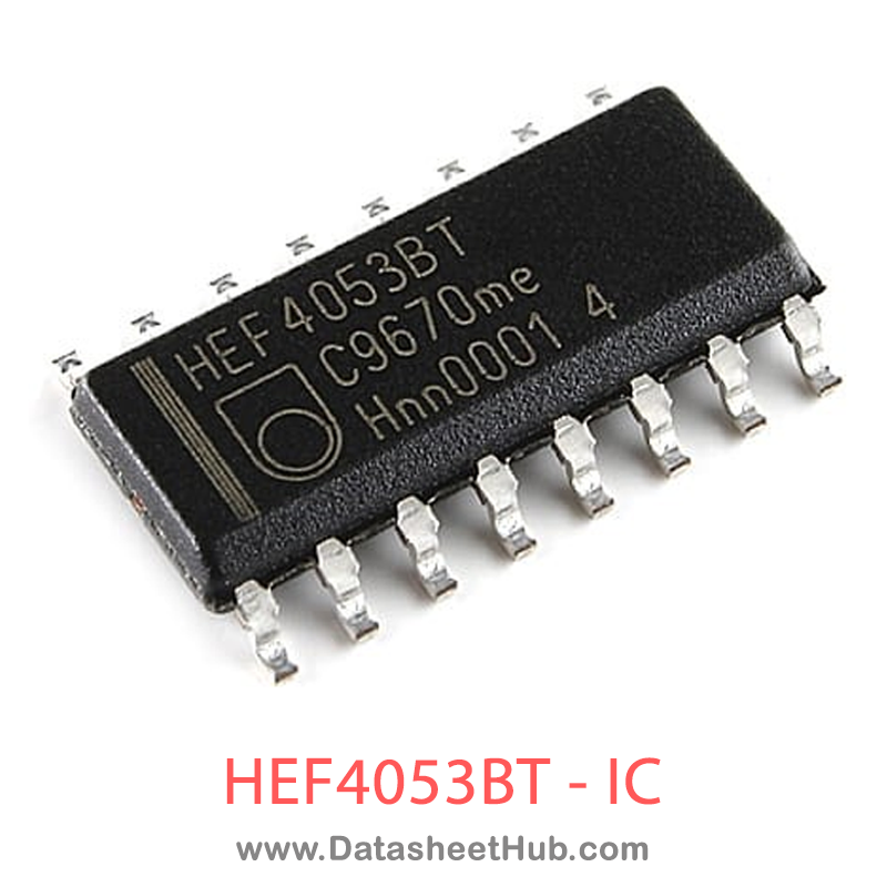
HEF4053BT overview
The HEF4053BT is a Triple 2-channel analogue multiplexer/demultiplexer made by Philips Electronics - NXP, supplied in these packages: SO16, DIP16, TSSOP16 type. The absolute maximum ratings table on this page lists the 11 limits from the manufacturer's datasheet that must not be exceeded. This page brings together the HEF4053BT pinout and maximum ratings, with the full datasheet PDF to preview below or download.
The HEF4053B is a triple single-pole double-throw (SPDT) analog switch, suitable for use as an analog or digital multiplexer/demultiplexer. Each switch has a digital select input (Sn), two independent inputs/outputs (nY0 and nY1) and a common input/output (nZ). All three switches share an enable input (E). A HIGH on E causes all switches into the high-impedance OFF-state, independent of Sn.
VDD and VSS are the supply voltage connections for the digital control inputs (Sn and E). The VDD to VSS range is 3 V to 15 V. The analog inputs/outputs (nY0, nY1 and nZ) can swing between VDD as a positive limit and VEE as a negative limit. VDD - VEE may not exceed 15 V. Unused inputs must be connected to VDD, VSS, or another input. For operation as a digital multiplexer/demultiplexer, VEE is connected to VSS (typically ground). VEE and VSS are the supply voltage connections for the switches.
Datasheet
HEF4053BT features
- Fully static operation
- 5 V, 10 V, and 15 V parametric ratings
- Standardized symmetrical output characteristics
- Specified from -40 °C to +125 °C
- Complies with JEDEC standard JESD 13-B
HEF4053BT pinout
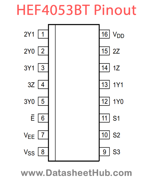
| Pin | Name | Description |
|---|---|---|
| 6 | E | enable input (active LOW) |
| 7 | VEE | supply voltage |
| 8 | VSS | ground supply voltage |
| 11, 10, 9 | S1, S2, S3 | select input |
| 12, 2, 5 | 1Y0, 2Y0, 3Y0 | independent input or output |
| 13, 1, 3 | 1Y1, 2Y1, 3Y1 | independent input or output |
| 14, 15, 4 | 1Z, 2Z, 3Z | independent output or input |
| 16 | VDD | supply voltage |
Absolute maximum ratings
| Parameter | Symbol | Value | Unit | Conditions |
|---|---|---|---|---|
| supply voltage | VDD | Min -0.5 / Max +18 | V | |
| supply voltage | VEE | Min -18 / Max +0.5 | V | referenced to VDD |
| input clamping current | IIK | Max ±10 | mA | pins Sn and E; VI < -0.5 V or VI > VDD + 0.5 V |
| input voltage | VI | Min -0.5 / Max VDD + 0.5 | V | |
| input/output current | II/O | Max ±10 | mA | |
| supply current | IDD | Max 50 | mA | |
| storage temperature | Tstg | Min -65 / Max +150 | °C | |
| ambient temperature | Tamb | Min -40 / Max +125 | °C | |
| - | SO16 package [2] | Min mW | 500 | |
| - | TSSOP16 package [2] | Min mW | 500 | |
| power dissipation | P | Max 100 | mW | per output |
HEF4053BT applications
- Analog multiplexing and demultiplexing
- Digital multiplexing and demultiplexing
- Signal gating
Comments 0
Leave a comment