

HS01G Datasheet – Half-Bridge Resonant Controller IC
HS01G, ICE1HS01G
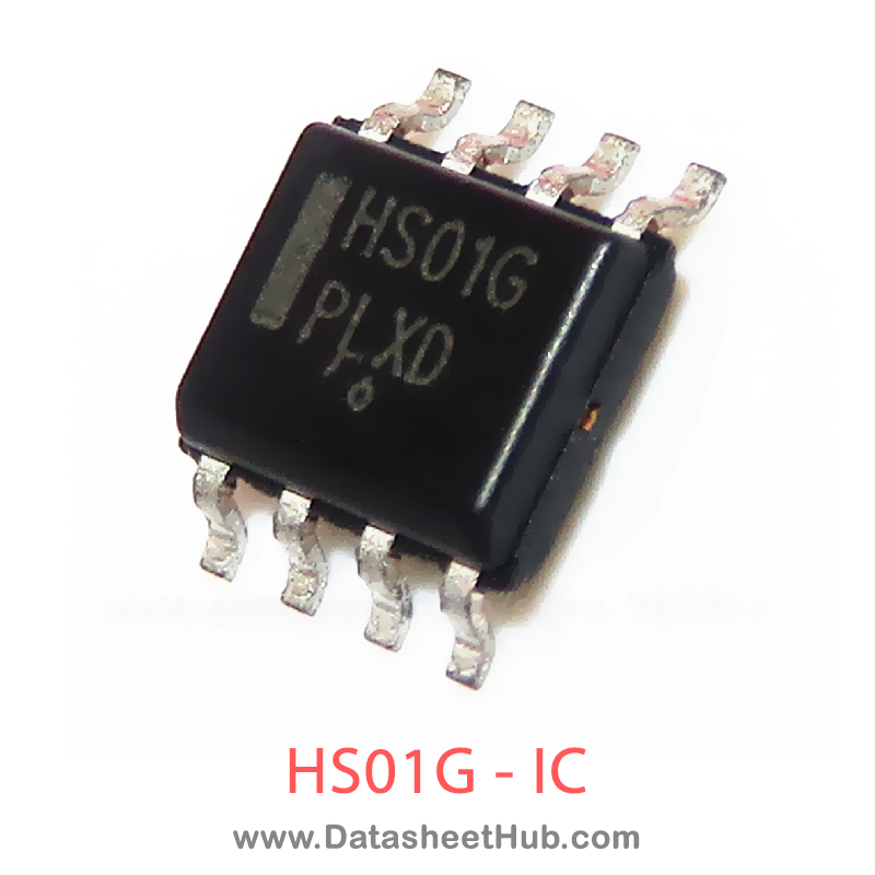
HS01G overview
The HS01G is an HS01G, ICE1HS01G made by Infineon Technologies AG, supplied in a Half-Bridge Resonant Controller package. The absolute maximum ratings table on this page lists the 12 limits from the manufacturer's datasheet that must not be exceeded. This page brings together the HS01G pinout and maximum ratings, with the full datasheet PDF to preview below or download.
The controller ICE1HS01G with two gate outputs is specially designed for LLC resonant half-bridge converters. An oscillator with accurately-programmed frequency range is built inside the IC. The two gate signals are obtained by passing the signal out from the oscillator through a divide-by-two flip-flop. Therefore, two signals are of exactly 50% duty cycle and 180o out of phase. To guarantee the zero-voltage-switching and safe operation in half-bridge topologies, a fixed dead time of 380ns is inserted in each internal when one switch is turned off and the other is turned on.
For LLC resonant half-bridge converter, the output voltage is regulated by changing the switching frequency. ICE1HS01G offers the designer to choose suitable operation frequency range by programming the oscillator with one single resistor. In addition, ICE1HS01G offers a programmed soft-start function to limit both the inrush current and the overshoot in output voltage. To protect the system during operation, mains input under-voltage protection and over-current protection are integrated in ICE1HS01G as well.
Datasheet
HS01G features
- 64Mb (8MB) Flash Memory
- High-Speed Data Read
- Wide Operating Voltage Range
- SPI Serial Interface
- Erase and Program Operations
- Non-Volatile Data Storage
- Reliable Data Retention
- Industrial Temperature Range
- Compact Package Design
- RoHS Compliance
HS01G pinout
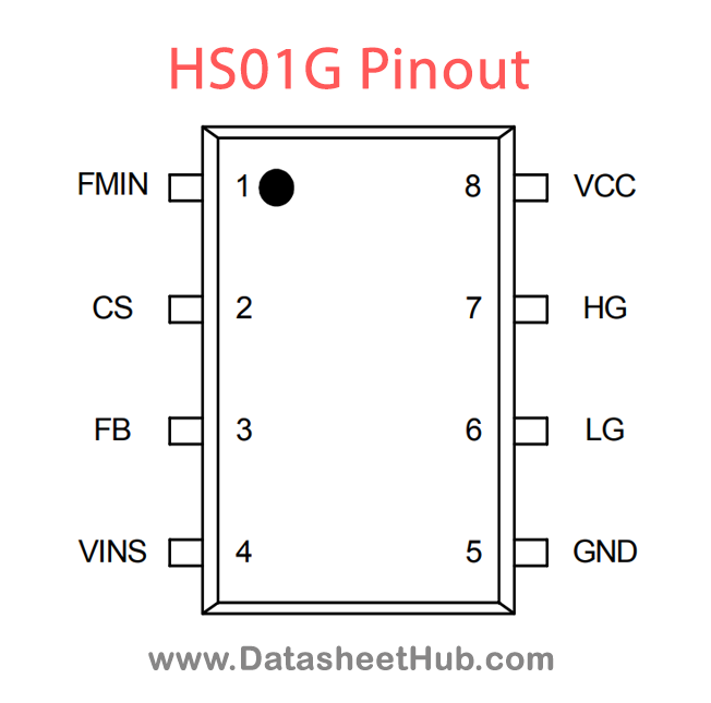
| Pin | Name | Description |
|---|---|---|
| 1 | FMIN | Minimum switching frequency |
| 2 | CS | Current sense |
| 3 | FB | Feedback voltage |
| 4 | VINS | Input voltage sense |
| 5 | GND | IC ground |
| 6 | LG | Low side gate drive |
| 7 | HG | High side gate drive |
| 8 | VCC | IC power supply |
Absolute maximum ratings
| Parameter | Symbol | Value | Unit |
|---|---|---|---|
| VCC Supply Voltage | VVCC | Min -0.3 / Max 20.51) | V |
| VHG Voltage | VLG | Min -0.3 / Max 18 | V |
| VLG Voltage | VLG | Min -0.3 / Max 18 | V |
| CS voltage | VCS | Min -0.3 / Max 5 | V |
| FB voltage | VFB | Min -0.3 / Max 5 | V |
| VINS voltage | VVINS | Min -0.3 / Max 5 | V |
| FMIN voltage | VFMIN | Min -0.3 / Max 5 | V |
| Maximum source current on FMIN | IFMIN | Max 2.5 | mA |
| Junction Temperature | Tj | Min -40 / Max 125 | °C |
| Storage Temperature | TS | Min -55 / Max 150 | °C |
| Thermal Resistance Junction-Ambient for PG-DSO-8 | RthJA(DSO) | Max 185 / Remarks PG-DSO-8 | K/W |
| ESD Capability | VESD | Max 2 / Remarks Human body model2) | kV |
HS01G applications
- Flash Memory Storage
- Microcontroller Code Storage
- Firmware Updates
- Data Logging Systems
- Embedded Systems
Comments 0
Leave a comment