

ISL95836 Datasheet – Dual 3+2 PWM Controller
Dual 3+2 PWM Controller for IMVP-7/VR12 CPUs
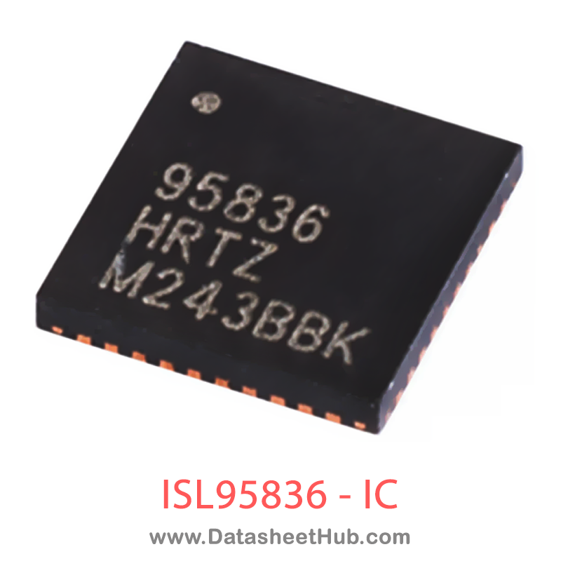
ISL95836 overview
The ISL95836 is a Dual 3+2 PWM Controller for IMVP-7/VR12 CPUs made by Intersil Corporation, supplied in a 40 Ld 5×5 TQFN Type package. The absolute maximum ratings table on this page lists the 9 limits from the manufacturer's datasheet that must not be exceeded. This page brings together the ISL95836 pinout and maximum ratings, with the full datasheet PDF to preview below or download.
Compliant with IMVP-7/VR12™, the ISL95836 provides a complete solution for microprocessor and graphic processor core power supply. It provides two Voltage Regulators (VRs) with three integrated gate drivers. The first VR can be configured as 3-, 2- or 1-phase VR while the second VR could be configured as 2- or 1-phase VR, providing maximum flexibility. The two VRs share the serial control bus to communicate with the CPU and achieve lower cost and smaller board area compared with the two-chip approach.
Based on Intersil’s Robust Ripple Regulator (R3) technology™, the PWM modulator compared to traditional modulators, has faster transient settling time, variable switching frequency during load transients and has improved light load efficiency with it’s ability to automatically change switching frequency.
The ISL95836 has several other key features. Both outputs support DCR current sensing with single NTC thermistor for DCR temperature compensation or accurate resistor current sensing. Both outputs come with remote voltage sense, programmable VBOOT voltage, IMAX and switching frequency, adjustable OC protection and separate Power-Good.
Datasheet
ISL95836 features
- Serial Data Bus
- Dual Outputs
- Configurable 3-, 2- or 1-phase for the 1st Output using 2 integrated Gate Drivers
- Configurable 2- or 1-phase for the 2nd Output using an Integrated Gate Driver
- 0.5% System Accuracy Over-Temperature
- Supports Multiple Current Sensing Methods
- Lossless Inductor DCR Current Sensing
- Precision Resistor Current Sensing
- Differential Remote Voltage Sensing
- Programmable VBOOT Voltage at Start-up
- Resistor Programmable IMAX, Switching Frequency for Both Outputs
- Adaptive Body Diode Conduction Time Reduction
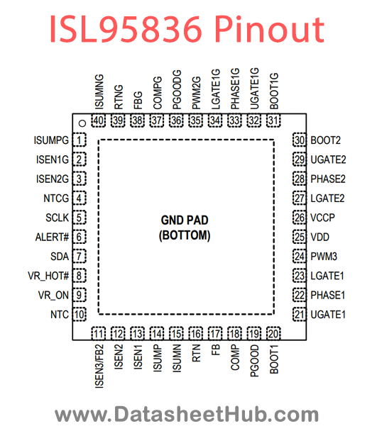
ISL95836 pinout
| Name | Description |
|---|---|
| BOTTOM PAD | Signal common of the IC. Unless otherwise stated, signals are referenced to the GND pin. In addition, it is the return path for all the low-side MOSFET gate drivers. It should also be used as the thermal pad for heat removal. |
| 1, 41 | VR2 droop current sense input. When ISUMNG is pulled to 5V VDD, all the communication to VR2 is disabled. |
| 2 | Individual current sensing for VR2 Phase 1. |
| 3 | Individual current sensing for VR2 Phase 2. When ISEN2 is pulled to 5V VDD, the controller will disable VR2 Phases 2. |
| 4 | The second thermistor input to VR_HOT# circuit. Use it to monitor VR2 temperature. |
| 5, 6, 7 | Communication bus between the CPU and the VRs. |
| 8 | Open drain thermal overload output indicator. Can be considered part of communication bus with CPU. |
| 9 | Controller enable input. A high level logic signal on this pin enables the controller. |
| 10 | One of the thermistor inputs to VR_HOT# circuit. Use it to monitor VR1 temperature. |
| 11 | When the VR1 is configured in 3-phase mode, this pin is ISEN3. ISEN3 is the individual current sensing for VR1 phase 3. When VR1 is configured in 2-phase mode, this pin is FB2. There is a switch between the FB2 pin and the FB pin. The switch is on when VR1 is in 2-phase mode and is off in 1- phase m |
| 12 | Individual current sensing for VR1 Phase 2. When ISEN2 and PWM3 are both pulled to 5V VDD, the controller will disable VR1 Phases 3 and 2. |
| 13 | Individual current sensing for VR1 Phase 1. |
Absolute maximum ratings
| Parameter | Value |
|---|---|
| Battery Voltage, VIN | +28V |
| Boot-to-Phase Voltage (BOOT-PHASE) -0.3V to +7V(DC) | 0.3V to +9V(<10ns) |
| Phase Voltage (PHASE) | -7V (<20ns Pulse Width, 10µJ) |
| UGATE Voltage (UGATE) | PHASE - 0.3V (DC) to BOOT |
| PHASE - 5V | (<20ns Pulse Width, 10µJ) to BOOT |
| LGATE Voltage | -2.5V (<20ns Pulse Width, 5µJ) to VDD+0.3V |
| All Other Pins | 0.3V to (VDD +0.3V) |
| ESD Rating Human Body Model (Tested per JESD22-A114E) Machine Model (Tested per JESD22-A115-A) Charged Device Model (Tested per JESD22-C101A) | KVV1K |
| Latch Up (Tested per JESD-78B; Class 2, Level A) | 100mA |
ISL95836 applications
- IMVP-7/VR12 Compliant Computers
- Laptop Computers
- Ultrabook
- Tablet Computers
- Industrial Computing
- Embedded Systems
Comments 0
Leave a comment