

LNK363 Datasheet – Low Power Off-Line Switcher IC

LNK363 overview
The LNK363 is a Low Power Off-Line Switcher IC made by Power Integrations, supplied in these packages: DIP, SO, SMD 8 Pin Type. The absolute maximum ratings table on this page lists the 5 limits from the manufacturer's datasheet that must not be exceeded. This page brings together the LNK363 pinout and maximum ratings, with the full datasheet PDF to preview below or download.
LinkSwitch™-XT incorporates a 700 V power MOSFET, oscillator, simple ON/OFF control scheme, a high-voltage switched current source, frequency jittering, cycle-by-cycle current limit and thermal shutdown circuitry onto a monolithic IC. The start-up and operating power are derived directly from the DRAIN pin, eliminating the need for a bias winding and associated circuitry.
Datasheet
LNK363 features
- Accurate hysteretic thermal shutdown protection – automatic recovery improves field reliability
- Universal input range allows worldwide operation
- Simple ON/OFF control, no loop compensation needed
- Eliminates bias winding – simpler, lower cost transformer
- Very low component count – higher reliability and single side printed circuit board
- Auto-restart reduces delivered power by 95% during short-circuit and open loop fault conditions
- High bandwidth provides fast turn-on with no overshoot and excellent transient load response
LNK363 pinout
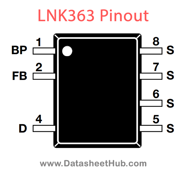
| Pin | Name | Description |
|---|---|---|
| D | DRAIN | Power MOSFET drain connection. Provides internal operating current for both start-up and steady-state operation. |
| BP | BYPASS | Connection point for a 0.1 mF external bypass capacitor for the internally generated 5.8 V supply. If an external bias winding is used, the current into the BP pin must not exceed 1 mA. |
| FB | FEEDBACK | During normal operation, switching of the power MOSFET is controlled by this pin. MOSFET switching is disabled when a current greater than 49 mA is delivered into this pin. |
| S | SOURCE | This pin is the power MOSFET source connection. It is also the ground reference for the BYPASS and FEEDBACK pins. |
Absolute maximum ratings
| Parameter | Value |
|---|---|
| Peak DRAIN Pin Current: LNK362 LNK363/364 | 200 mA (375 mA)(2) 400 mA (750 mA)(2) |
| FEEDBACK Pin Current | 100 mA |
| Storage Temperature | -65 °C to 150 °C |
| Operating Junction Temperature (3) | -40 °C to 150 °C |
| Lead Temperature (4) | 260 °C |
LNK363 applications
- Chargers/adapters for cell/cordless phones, PDAs, digital cameras, MP3/portable audio players, and shavers
- Supplies for appliances, industrial systems, and metering
Comments 0
Leave a comment