

M29F400 Datasheet – 4 Mbit, Single Supply Flash Memory
4 Mbit ( 512Kb x8 or 256Kb x16 ) / Boot Block Single Supply Flash Memory
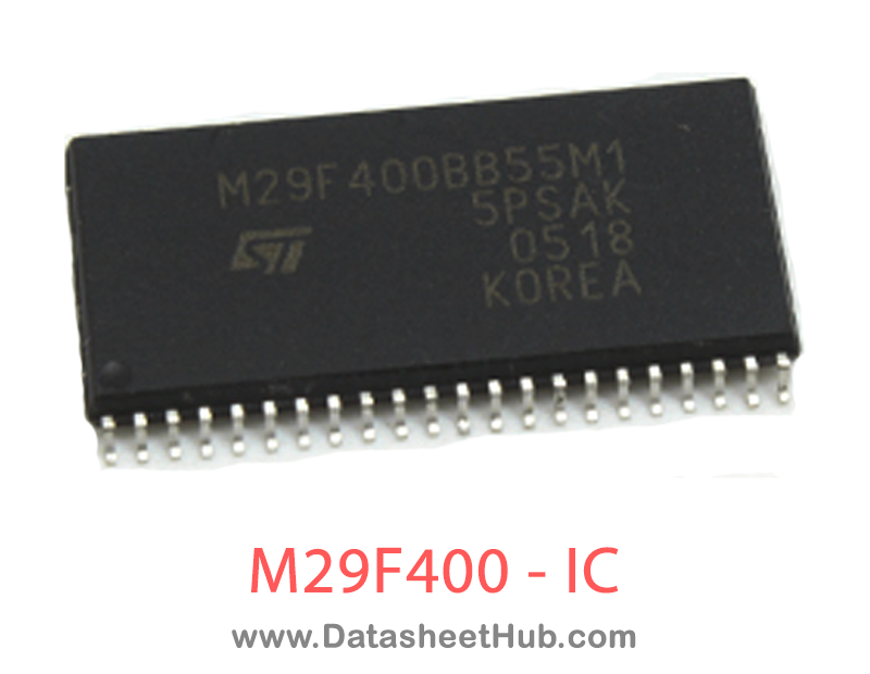
M29F400 overview
The M29F400 is a 4 Mbit ( 512Kb x8 or 256Kb x16 ) / Boot Block Single Supply Flash Memory made by STMicroelectronics, supplied in these packages: TSOP 48, SO44 Pin Type. The absolute maximum ratings table on this page lists the 5 limits from the manufacturer's datasheet that must not be exceeded. This page brings together the M29F400 pinout and maximum ratings, with the full datasheet PDF to preview below or download.
The M29F400 is a non-volatile memory that may be erased electrically at the block or chip level and programmed in-system on a Byte-by-Byte or Word- by-Word basis using only a single 5V VCC supply. For Program and Erase operations the necessary high voltages are generated internally. The device can also be programmed in standard programmers.
The array matrix organization allows each block to be erased and reprogrammed without affecting other blocks. Blocks can be protected against programing and erase on programming equipment, and temporarily unprotected to make changes in the application.
Instructions for Read/Reset, Auto Select for reading the Electronic Signature or Block Protection status, Programming, Blockand Chip Erase, Erase Suspend and Resume are written to the device in cyclesof commands to a Command Interface using standard microprocessor write timings.
The device is offered in TSOP48 (12 x 20mm) and SO44 packages. Both normal and reverse pinouts are available for the TSOP48 package.
Datasheet
M29F400 features
- M29F400T and M29F400B are replaced respectively by the M29F400BT and M29F400BB
- 5V±10% SUPPLY VOLTAGE for PROGRAM, ERASE and READ OPERATIONS
- FAST ACCESS TIME: 55ns FAST PROGRAMMING TIME 10ms by Byte / 16ms by Word typical
- 10ms by Byte / 16ms by Word typical
- PROGRAM/ERASE CONTROLLER (P/E.C.)
- Program Byte-by-Byte or Word-by-Word
- Status Register bits and Ready/Busy Output
- MEMORY BLOCKS Boot Block (Top or Bottom location) Parameter and Main blocks
- Boot Block (Top or Bottom location)
- Parameter and Main blocks
- BLOCK, MULTI-BLOCK and CHIP ERASE
- MULTI-BLOCK PROTECTION/TEMPORARY UNPROTECTION MODES
- ERASE SUSPEND and RESUME MODES Read and Program another Block during Erase Suspend
- Read and Program another Block during Erase Suspend
- LOW POWER CONSUMPTION Stand-by and Automatic Stand-by
- Stand-by and Automatic Stand-by
- 100,000 PROGRAM/ERASE CYCLES per BLOCK
- 20 YEARS DATA RETENTION Defectivity below 1ppm/year
- Defectivity below 1ppm/year
- ELECTRONIC SIGNATURE
- Manufacture Code 0020h
- Device Code M29F400T : 00D5h
- Device Code M29F400B : 00D6h
M29F400 pinout
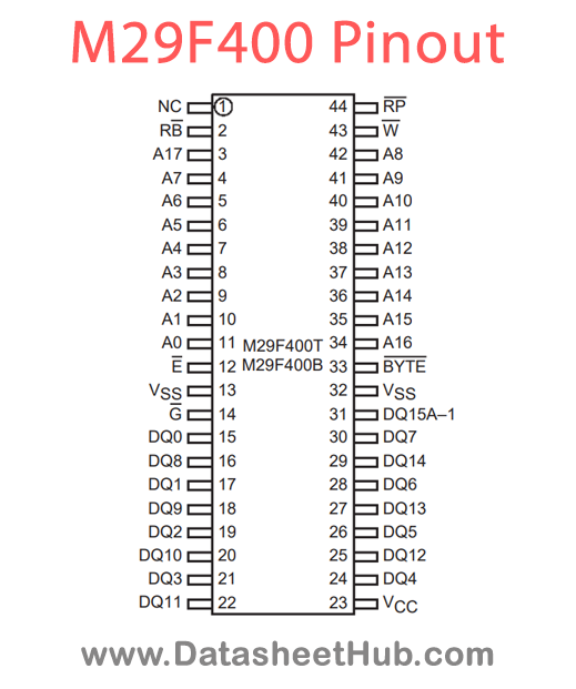
| Name | Description |
|---|---|
| A0 - A17 | Address Inputs |
| DQ0 - DQ7 | Data Input/Outputs, Command Inputs |
| DQ8 - DQ14 | Data Input/Outputs |
| DQ15A_1 | Data Input/Output or Address Input |
| E | Chip Enable |
| G | Output Enable |
| W | Write Enable |
| RP | Reset / Block Temporary Unprotect |
| RB | Ready/Busy Output |
| BYTE | Byte/Word Organization |
| Vss | Supply Voltage |
| Vss | Ground |
Absolute maximum ratings
| Parameter | Symbol | Value | Unit |
|---|---|---|---|
| Ambient Operating Temperature (3) | TA | –40 to 125 | °C |
| Temperature Under Bias | TBIAS | –50 to 125 | °C |
| Storage Temperature Input or Output Voltages | TSTG VIO (2) | –65 to 150 –0.6 to 7 | °C V |
| Supply Voltage | VCC | –0.6 to 7 | V |
| A9, E, G, RP Voltage | V(A9, E, G, RP) (2) | –0.6 to 13.5 | V |
M29F400 applications
- Flash Memory for Microcontrollers
- Embedded Systems
- Storage in Consumer Electronics
- Automotive Control Systems
Comments 0
Leave a comment