
MB39A132 Datasheet – Rectification DC/DC Converter IC
Synchronous Rectification DC/DC Converter IC
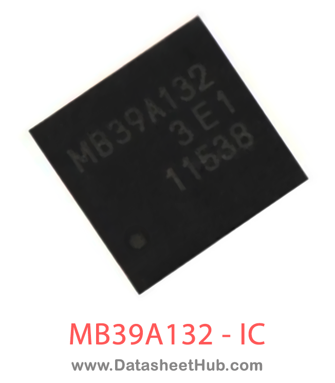
MB39A132 overview
The MB39A132 is a Synchronous Rectification DC/DC Converter IC, supplied in a QFN 32 Pin Type package. The absolute maximum ratings table on this page lists the 14 limits from the manufacturer's datasheet that must not be exceeded. This page brings together the MB39A132 pinout and maximum ratings, with the full datasheet PDF to preview below or download.
MB39A132, which is used for charging Li-ion battery, is a synchronous rectification DC/DC converter IC adopting pulse width modification (PWM). It can control charge voltage and charge current separately and supports the N-ch MOS driver. In addition, MB39A132 is suitable for down-conversion.
MB39A132 has an AC adapter detection comparator, which is independent of the DC/DC converter control block, and can control the source supplying voltage to the system. MB39A132 supports a wide input voltage range, enables low current consumption in standby mode, and can control the charge voltage and charge current with high precision, which is perfect for the built-in Li-ion battery charger used in devices such as notebook PC.
Datasheet
MB39A132 features
- Supports 2/3/4-Cell battery pack
- Two built-in constant current control loops
- Built-in AC adapter detection function (ACOK pin)
- Charge voltage setting accuracy: ±0.5% (Ta = + 25 °C to + 85 °C)
- Charge voltage control setting can be selected without using any external resistor. (4.00 V/Cell, 4.20 V/ Cell, 4.35 V/Cell)
- Output voltage can also be freely set by using the external resistor.
- Two built-in high-precision current detection amplifiers
- :Input offset voltage:+3 mV
- :Detection accuracy: ±1 mV (+INC1, +INC2 = 3 V to VCC)
- Charge current control setting can be selected without using any external resistor. (RS = 20 mL: 2.85 A) Charge current can also be freely set by using the external resistor.
- Switching frequency can be set by using the external resistor (MB39A132 has a built-in frequency setting capacitor.):100 kHz to 2 MHz
- Built-in off time control function
- In standby mode (Icc = 6 mA Typ), only the AC adapter detection function is in operation.
- Built-in output stage for N-ch MOS FET synchronous rectification
- Built-in charge stop function at low VCC pin voltage
- Built-in soft-start function whose setting time can be adjusted
- Equipped with the function enabling the independent operation of the AC adapter current detection amplifier
- Package: QFN-32
MB39A132 pinout
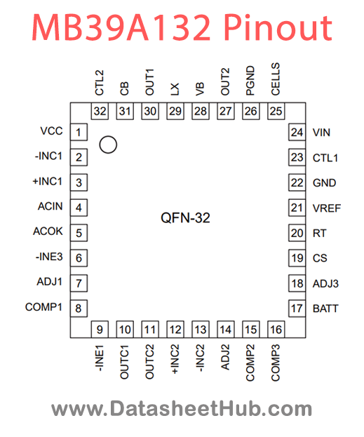
| Pin | Name | Description |
|---|---|---|
| 1 | VCC | Power supply pin for reference power and control circuit (Battery side). |
| 2 | -INC1 | Current detection amplifier (Current Amp1) inverted input pin. |
| 3 | +INC1 | Current detection amplifier (Current Amp1) non-inverted input pin. |
| 4 | ACIN | AC adapter voltage detection block (AC Comp.) input pin. |
| 5 | ACOK | AC adapter voltage detection block (AC Comp.) output pin. ACOK = Lo-Z when ACIN = H, ACOK = Hi-Z when ACIN = L |
| 6 | -INE3 | Error amplifier (Error Amp3) inverted input pin. |
| 7 | ADJ1 | Error amplifier (Error Amp1) non-inverted input pin. |
| 8 | COMP1 | Error amplifier (Error Amp1) output pin. |
| 9 | -INE1 | Error amplifier (Error Amp1) inverted input pin. |
| 10 | OUTC1 | Current detection amplifier (Current Amp1) output pin. |
| 11 | OUTC2 | Current detection amplifier (Current Amp2) output pin. |
| 12 | +INC2 | Current detection amplifier (Current Amp2) non-inverted input pin. |
| 13 | -INC2 | Current detection amplifier (Current Amp2) inverted input pin. |
| 14 | ADJ2 | Input pin for the charge current control block. ADJ2 pin “GND to 4.4 V” :Charge current control block output = ADJ2 pin voltage ADJ2 pin “4.6 V to VREF” :Charge current control block output = 1.5 V |
| 15 | COMP2 | Error amplifier (Error Amp2) output pin. |
| 16 | COMP3 | Error amplifier (Error Amp3) output pin. |
| 17 | BATT | Charge voltage control block battery voltage input pin. |
| 18 | ADJ3 | Charge voltage control block setting input pin. ADJ3 pin “GND” :Charge voltage 4.00 V/Cell ADJ3 pin “1.1 V to 2.2 V” :Charge voltage 2 ´ ADJ3 pin voltage/Cell ADJ3 pin “2.4 V to 3.9 V” :Charge voltage 4.35 V/Cell ADJ3 pin “4.1 V to VREF” :Charge voltage 4.20 V/Cell |
| 19 | CS | Soft-start capacitor connection pin. |
| 20 | RT | Triangular wave oscillation frequency setting resistor connection pin. |
| 21 | VREF | Reference voltage output pin. |
| 22 | GND | Ground pin. |
| 23 | CTL1 | Power supply control pin. When the CTL1 pin is set to “H” level, the DC/DC converter becomes operable. When the CTL1 pin is set to “L” level, the DC/DC converter becomes stand-by. |
| 24 | VIN | Power supply pin for ACOK function and Current Amp1(AC adapter side). |
Show all 32 pins
| Pin | Name | Description |
|---|---|---|
| 25 | CELLS | Charge voltage setting switch pin (2/3/4-Cell). CELLS = VREF: 4 Cells, CELLS = OPEN: 3 Cells, CELLS = GND: 2 Cells |
| 26 | PGND | Ground pin. |
| 27 | OUT2 | External low-side FET gate drive pin. |
| 28 | VB | FET drive circuit power supply pin. |
| 29 | LX | External high-side FET source connection pin. |
| 30 | OUT1 | External high-side FET gate drive pin. |
| 31 | CB | Boot strap capacitor connection pin. The capacitor is connected between the CB pin and the LX pin. |
| 32 | CTL2 | Power supply control pin for Current Amp1.When the CTL1 pin is set to “H” level, the DC/DC converter becomes operable. When the CTL1 pin is set to “L” level, the DC/DC converter becomes stand-by. |
Absolute maximum ratings
| Parameter | Symbol | Value | Unit | Conditions |
|---|---|---|---|---|
| Power supply voltage | VVCC | Min - 0.3 / Max + 27 | V | VCC pin |
| VVIN | VIN pin | Min + 27 / Max V | - 0.3 | |
| CB pin input voltage | VCB | Min - 0.3 / Max + 32 | V | CB pin |
| CTL1, CTL2 pin input voltage | VCTL | Min - 0.3 / Max + 27 | V | CTL1, CTL2 pins |
| Input voltage | VINC | Min - 0.3 / Max + 27 | V | -INC1, +INC1 pins |
| -INC2, +INC2, BATT pins | - 0.3 | Min V | + 20 | |
| VADJ | ADJ1, ADJ2, ADJ3, CELLS pins | Min VVREF + 0.3 / Max V | - 0.3 | |
| VINE | -INE1, -INE3 pins | Min VVREF + 0.3 / Max V | - 0.3 | |
| ACIN input voltage | VACIN | Min - 0.3 / Max VVIN | V | ACIN pin |
| ACOK pin output voltage | VACOK | Min - 0.3 / Max + 27 | V | ACOK pin |
| Output current | IOUT | Min - 60 / Max + 60 | mA | OUT1, OUT2 pins |
| Power dissipation | PD | Min ¾ / Max 4400*1,*2,*3 | mW | Ta £ + 25 °C |
| Ta = + 85 °C | ¾ | Min mW | 1760*1,*2,*3 | |
| Storage temperature | TSTG | Min - 55 / Max + 125 | °C | ¾ |
MB39A132 applications
- Internal charger used in notebook PC
- Handy terminal device etc.
Comments 0
Leave a comment