

MP1482 Datasheet – Step-Down Converter
2A 18V Synchronous Rectified Step-Down Converter
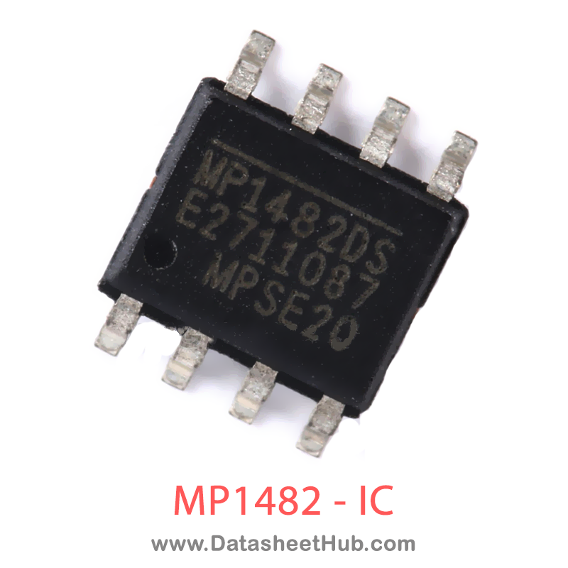
MP1482 overview
The MP1482 is a 2A 18V Synchronous Rectified Step-Down Converter made by Monolithic Power Systems, supplied in an SOP 8 Pin Type package. The absolute maximum ratings table on this page lists the 5 limits from the manufacturer's datasheet that must not be exceeded. This page brings together the MP1482 pinout and maximum ratings, with the full datasheet PDF to preview below or download.
The MP9141 is a monolithic step-down switch mode regulator with a built in internal power MOSFET. It achieves 1.8A continuous output current over a wide input supply range with excellent load and line regulation.
Current mode operation provides fast transient response and eases loop stabilization.
Fault condition protection includes cycle-by-cycle current limiting and thermal shutdown. In shutdown mode the regulator draws 25μA of supply current.
The MP9141 requires a minimum number of readily available standard external components.
Datasheet
MP1482 features
- 1.8A Output Current
- 0.25Ω Internal Power MOSFET Switch
- Stable with Low ESR Output Ceramic Capacitors
- Up to 92% Efficiency
- 25µA Shutdown Mode
- Fixed 380KHz Frequency
- Thermal Shutdown
- Cycle-by-Cycle Over Current Protection
- Wide 4.75V to 20V Operating Input Range
- Output Adjustable from 1.22V to 12V
- Programmable Under Voltage Lockout
- Available in an 8-Pin SOIC Package
MP1482 pinout
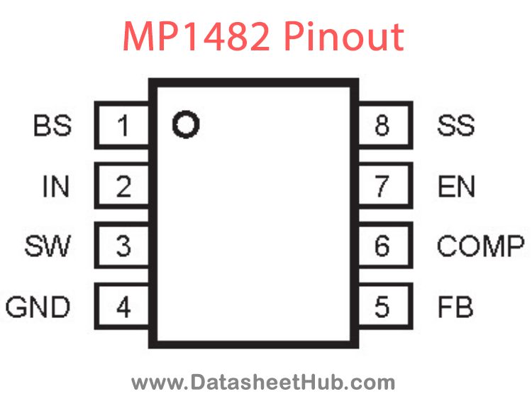
| Pin | Name | Description |
|---|---|---|
| 1 | BS | High-Side Gate Drive Boost Input. BS supplies the drive for the high-side N-Channel MOSFET switch. Connect a 10nF or greater capacitor from SW to BS to power the switch. |
| 2 | IN | Power Input. IN supplies the power to the IC, as well as the step-down converter switch. Drive IN with a 4.75V to 20V power source. Bypass IN to GND with a suitably large capacitor to eliminate noise on the input to the IC. See Input Capacitor. |
| 3 | SW | Power Switching Output. SW is the switching node that supplies power to the output. Connect the output LC filter from SW to the output load. Note that a capacitor is required from SW to BS to power the high-side switch. |
| 4 | GND | Ground. |
| 5 | FB | Feedback Input. FB senses the output voltage and regulates it. Drive FB with a resistive voltage divider from the output voltage. The feedback threshold is 1.222V. See Setting the Output Voltage. |
| 6 | COMP | Compensation Node. COMP is used to compensate the regulation control loop. Connect a series RC network from COMP to GND to compensate the regulation control loop. See Compensation. |
| 7 | EN | Enable Input. EN is a digital input that turns the regulator on or off. Drive EN high to turn on the regulator, low to turn it off. For automatic startup, leave EN unconnected. |
| 8 | NC | No Connect. |
Absolute maximum ratings
| Parameter | Value |
|---|---|
| Boot Strap Voltage (VBS) .VSW | – 0.3V to VSW + 6V |
| Continuous Power Dissipation (TA = +25°C) (2) | 1.4W |
| Junction Temperature | 150°C |
| Lead Temperature | 260°C |
| Storage Temperature | 65°C to +150°C |
MP1482 applications
- PC Monitors
- Distributed Power Systems
- Battery Charger
- Pre-Regulator for Linear Regulators
Comments 0
Leave a comment