

OPA192 Datasheet – Precision Operational Amplifier
High Voltage, Rail-to-Rail Input/Output, Precision Operational Amplifier
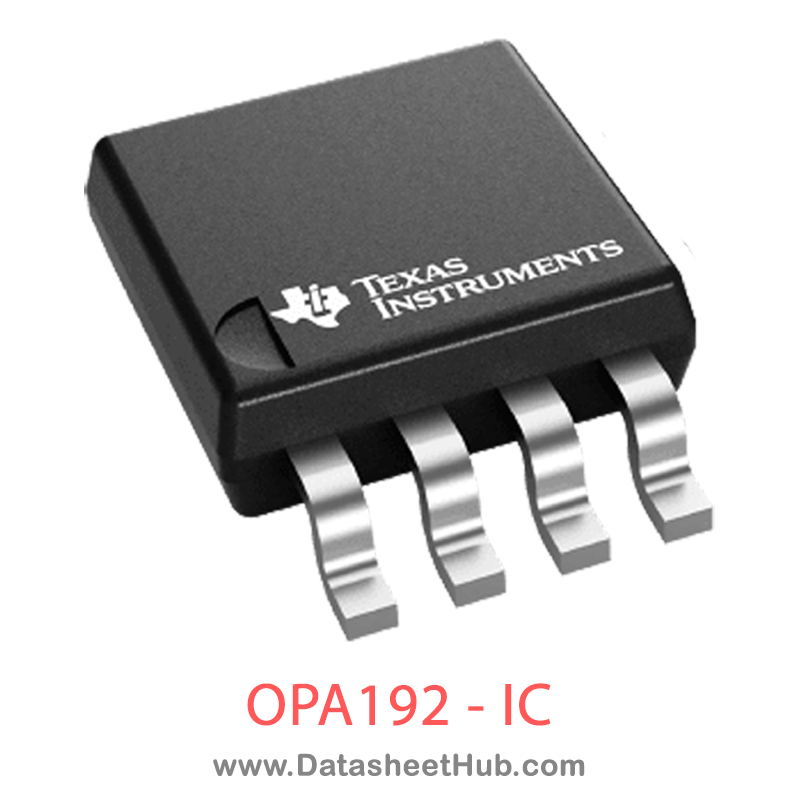
OPA192 overview
The OPA192 is a High Voltage, Rail-to-Rail Input/Output, Precision Operational Amplifier made by Texas Instruments, supplied in these packages: SOIC, SOT-23, VSSOP tpe. Main ratings: Low Offset Voltage ±5 µV; Low Offset Voltage Drift ±0.2 µV/°C; Low Noise 5.5 nV/√Hz at 1 kHz; High Common-Mode Rejection 140 dB. The absolute maximum ratings table on this page lists the 8 limits from the manufacturer's datasheet that must not be exceeded. This page brings together the OPA192 pinout, key specifications and maximum ratings, with the full datasheet PDF to preview below or download.
The OPAx192 family (OPA192, OPA2192, and OPA4192) is a new generation of 36-V, e-trim operational amplifiers.
These devices offer outstanding dc precision and ac performance, including rail-to-rail input/output, low offset (±5 µV, typ), low offset drift (±0.2 µV/°C, typ), and 10-MHz bandwidth.
Unique features such as differential input-voltage range to the supply rail, high output current (±65 mA), high capacitive load drive of up to 1 nF, and high slew rate (20 V/µs) make the OPA192 a robust, high-performance operational amplifier for high-voltage industrial applications
The OPA192 family of op amps is available in standard packages and is specified from –40°C to +125°C.
Key specifications
Datasheet
OPA192 features
- Rail-to-Rail Input and Output and 10-MHz bandwidth.
- EMI/RFI Filtered Inputs
- Differential Input Voltage Range to Supply Rail
- Industry Standard Packages
- standard packages and is specified from –40°C to +125°C.
- Single in SOIC-8, SOT-23-5, and VSSOP-8
- Dual in SOIC-8 and VSSOP-8
- Quad in SOIC-14 and TSSOP-14
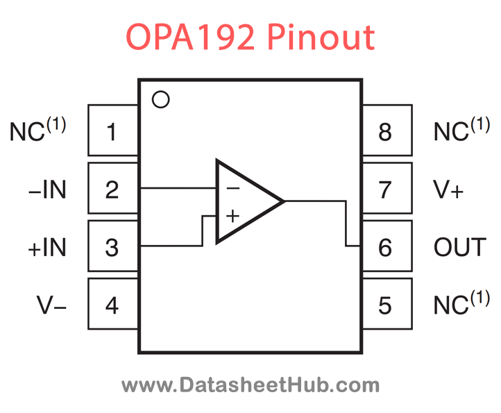
OPA192 pinout
| Name | Description |
|---|---|
| +IN | Noninverting input |
| –IN | Inverting input |
| NC | No internal connection (can be left floating) |
| OUT | Output |
| V+ | Positive (highest) power supply |
| V– | Negative (lowest) power supply |
Absolute maximum ratings
| Parameter | Value | Unit |
|---|---|---|
| Supply voltage, VS = (V+) – (V–) | Min ±20 (40, single supply) / Max V | |
| Signal input pins | Min Voltage / Max Common-mode | (V–) – 0.5 |
| Differential | Min (V+) – (V–) + 0.2 | |
| Current | Min ±10 / Max mA | |
| Output short circuit (2) | Min Continuous | |
| Temperature | Min Operating range / Max –55 | 150 |
| Junction | Min 150 | |
| Storage, Tstg | Min –65 / Max 150 |
OPA192 applications
- Multiplexed Data-Acquisition Systems
- Test and Measurement Equipment
- High-Resolution ADC Driver Amplifiers
- SAR ADC Reference Buffers
- Programmable Logic Controllers
- High-Side and Low-Side Current Sensing
- High Precision Comparator
Comments 0
Leave a comment