
SL1925 Datasheet – Satellite Zero IF QPSK Tuner IC
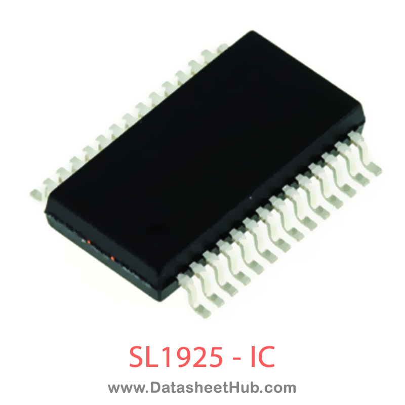
SL1925 overview
The SL1925 is a Satellite Zero IF QPSK Tuner IC, supplied in an SSOP 28 Pin Type package. The absolute maximum ratings table on this page lists the 10 limits from the manufacturer's datasheet that must not be exceeded. This page brings together the SL1925 pinout and maximum ratings, with the full datasheet PDF to preview below or download.
The SL1925 is a wideband quadrature converter operating from 950 to 2150 MHz, intended primarily for application in satellite tuners.
The device contains all elements necessary, with the exception of local oscillator sustaining network, to fabricate a high performance I(n-phase) & Q(uadrature) phase splitter and downconverter optimizer for systems containing RF AGC gain control. The device allows for systems containing higher power analog interferers. For most applications RF tunable filtering is not essential.
The SL1925 is optimizer for use with a low phase noise synthesizer, a range of which are available from Mitel Semiconductor. This will form a complete front end tuner function for digital satellite receiver systems utilizing DSP derogation recovery. The device includes a very high signal handling front end with AGC, this provides for gain control, reference local oscillator with output buffer, phase splitter with I and Q mixers and baseband buffer amplifiers with external interstage filtering.
Datasheet
SL1925 features
- Single chip system for direct quadrature down conversion from L-band
- High signal handling capability for minimum external component count application, requires external RF AGC of 30dB
- Compatible with DSS and DVB system requirements
- Excellent gain and phase match up to 30MHz baseband
- High output referred linearity for low distortion and multi channel application
- Fully balanced low radiation design
- Integral RF AGC amplifier
- Two selectable varactor tuned local oscillators with buffered output for driving external synthesiser loop
- ESD protection (Normal ESD handling procedures should be observed)
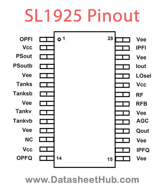
SL1925 pinout
Absolute maximum ratings
| Parameter | Value | Unit | Conditions |
|---|---|---|---|
| Supply Voltage, Vcc | Pins 2,13,23 / Minimum -0.3 / Maximum 7 | V | Transient condition only |
| PSout &PSoutb DC offset | Pins 3,4 / Minimum Vcc-3.0 / Maximum Vcc+0.3 | Vp-p | |
| RF & RFB input voltage | Pins 21,22 / Maximum 2.5 | Vp-p | AC coupled, transient conditions only |
| All other I/O ports DC offset | Pins 1,6,7,9 / Minimum -0.3 / Maximum Vcc+0.3 | V | |
| Storage Temperature | Minimum -55 / Maximum +150 | °C | |
| Junction Temperature | Maximum +150 | °C | |
| Chip to ambient | Maximum 85 | C/W | |
| Chip to case | Maximum 20 | C/W | |
| Power consumption at 5.25V | Maximum 893 | mW | |
| ESD protection | Pins All / Minimum 4 | kV | Mil Std-883 latest revision method 3015 |
SL1925 applications
- Satellite receiver systems
- Data communications systems
Comments 0
Leave a comment