

SN65LVDS311 Datasheet – 27 Bit Display Transmitter
Programmable 27 Bit Display Serial Interface Transmitter
SN65LVDS311 overview
The SN65LVDS311 is a Programmable 27 Bit Display Serial Interface Transmitter made by Texas Instruments, supplied in a DSBGA 49 Pin Type package. The absolute maximum ratings table on this page lists the 6 limits from the manufacturer's datasheet that must not be exceeded. This page brings together the SN65LVDS311 pinout and maximum ratings, with the full datasheet PDF to preview below or download.
The SN65LVDS311 serialize transmits 27 parallel input data over 1, 2, or 3 serial output links. The device pinout is optimized to interface with the OMAP3630 application processor. The device loads a shift register with the 24 pixel bits and 3 control bits from the parallel CMOS input interface. The data are latched into the device by the pixel clock, PCLK. In addition to the 27 bits, the device adds a parity bit and two reserved bits for a total number of 30 serial bits. The parity bit allows a receiver to detect single- bit errors. Odd parity is implemented.
The serial shift register is uploaded through 1, 2, or 3 serial outputs at 30, 15, or 10 times the pixel clock data rate. A copy of the pixel clock is output on an additional differential output. The serial data and clock are transmitted via Sub Low-Voltage Differential Signaling (SubLVDS) lines. The SN65LVDS311 supports three power modes (Shutdown, Standby and Active) to conserve power.
Datasheet
SN65LVDS311 features
- 2.8 × 2.8mm package size
- 1.8V input signal swing
- 24-Bit RGB Data, 3 Control Bits, 1 Parity Bit and 2 Reserved Bits Transmitted over 1, 2 or 3 Differential Lines
- SubLVDS Differential Voltage Levels
- Three Operating Modes to Conserve Power
- Active-Mode QVGA 17.4mW (typ)
- Active-Mode VGA 28.8mW (typ)
- Shutdown Mode ≈ 0.5μA (typ)
- Standby Mode ≈ 0.5μA (typ)
- ESD Rating > 3kV (HBM)
- Pixel Clock Range of 4MHz–65MHz
- Failsafe on all CMOS Inputs
- Typical Application: Cameras, Embedded Computers
SN65LVDS311 pinout
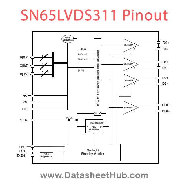
| Name | Description |
|---|---|
| D0+, D0– | SubLVDS Data Link (active during normal operation) |
| D1+, D1– | |
| D2+, D2– | |
| CLK+, CLK– | |
| R0–R7 | Red Pixel Data (8); pin assignment depends on SWAP pin setting |
| G0–G7 | |
| B0–B7 | |
| HS | |
| VS | |
| DE | |
| PCLK | |
| LS0, LS1 | |
| TXEN | |
| VDD | Supply Voltage |
| GND | |
| VDDLVDS | |
| GNDLVDS | |
| VDDPLLA | |
| GNDPLLA | |
| VDDPLLD | |
| GNDPLLD |
Absolute maximum ratings
| Parameter | Value | Unit |
|---|---|---|
| Supply voltage range, VDD (2), VDDPLLA, VDDPLLD, VDDLVDS | -0.3 to 2.175 | V |
| Voltage range at any input or output terminal | When VDDx > 0 V | -0.5 to 2.175 |
| When VDDx ≤ 0 V | -0.5 to VDD + 2.175 | V |
| Electrostatic discharge | Human Body Model (3) (all Pins) | ±3 |
| Charged-Device Mode (4) l (all Pins) | ±500 | V |
| Machine Model (5) (all pins) | ±200 |
SN65LVDS311 applications
- Flat-Panel Displays
- LCD Monitors
- Digital Signage
- Laptop and Notebook Screens
- Mobile Devices
Comments 0
Leave a comment