

SY8208CQNC Datasheet – Synchronous Step Down Regulator
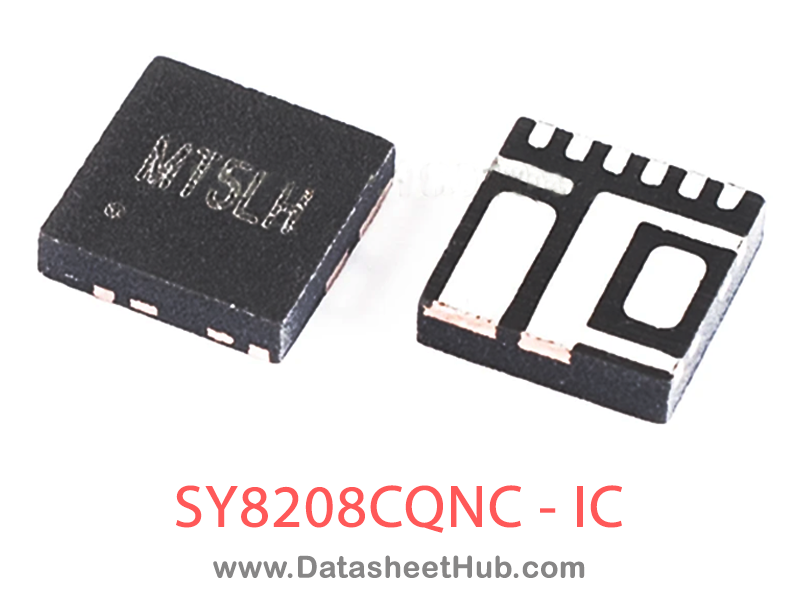
SY8208CQNC overview
The SY8208CQNC is a Synchronous Step Down Regulator made by Silergy, supplied in a QFN3x3-10 Pin Type package. The absolute maximum ratings table on this page lists the 8 limits from the manufacturer's datasheet that must not be exceeded. This page brings together the SY8208CQNC pinout and maximum ratings, with the full datasheet PDF to preview below or download.
The SY8208A develops a high efficiency synchronous step-down DC-DC regulator capable of delivering 8A continuous, 16A peak current. The SY8208A operates over a wide input voltage range from 4V to 28V and integrates main switch and synchronous switch with very low RDS(ON) to minimize the conduction loss.
The SY8208A adopts the instant PWM architecture to achieve fast transient responses for high step down applications and high efficiency at light loads. In addition, it operates at pseudo-constant frequency of 800kHz under continuous conduction mode to minimize the size of inductor and capacitor.
Datasheet
SY8208CQNC features
- Low RDS(ON) for internal switches (top/bottom): 20/10 mΩ
- Wide input voltage range: 4-28V
- Instant PWM architecture to achieve fast transient responses
- Internal 400uS soft start limits the inrush current
- Pseudo-constant frequency: 800kHz.
- 8A continuous/16A peak output current capability
- ±1.5% 0.6V reference
- Programmable peak current limit
- Power good indicator
- Output discharge function
- Short circuit latch off protection
- Over voltage latch off protection
- Input UVLO
- Over temperature protection
- RoHS Compliant and Halogen Free
- Compact package: QFN3x3-10
SY8208CQNC pinout
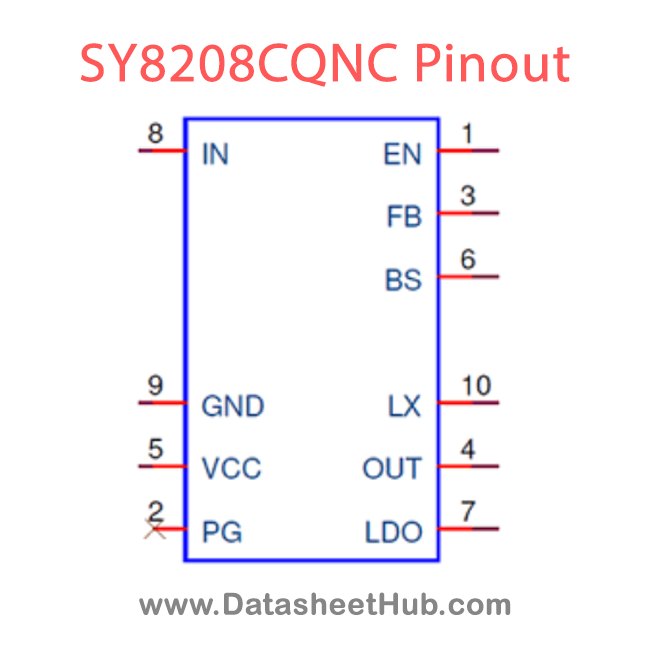
| Pin | Name | Description |
|---|---|---|
| 1 | EN | Enable control. Pull this pin high to turn on the IC. Do not leave this pin floating. |
| 2 | PG | Power good Indicator. Open drain output when the output voltage is within 90% to 120% of regulation point. |
| 3 | ILMT | Current limit setting pin. The current limit is set to 8A, 12A or 16A when this pin is pull low, floating or pull high respectively. |
| 4 | FB | Output Feedback Pin. Connect this pin to the center point of the output resistor divider (as shown in Figure 1) to program the output voltage: Vout=0.6*(1+R1/R2) |
| 5 | VCC | Internal 3.3V LDO output. Power supply for internal analog circuits and driving circuit. Bypass a capacitor to GND. |
| 6 | BS | Boot-Strap Pin. Supply high side gate driver. Decouple this pin to LX pin with 0.1uF ceramic cap. |
| 7,8 | IN | Input pin. Decouple this pin to GND pin with at least 10uF ceramic cap |
| 9 | GND | Ground pin |
| 10 | LX | Inductor pin. Connect this pin to the switching node of inductor |
Absolute maximum ratings
| Parameter | Value |
|---|---|
| IN, LX, PG, EN | 30V |
| BS-LX, FB, ILMT, VCC | 4V |
| Power Dissipation, PD @ TA = 25°C QFN3x3-10 - | -3.3W |
| Package Thermal Resistanceθ JAθ JC | 30°C/W4°C/W |
| Junction Temperature Range - | 125°C |
| Lead Temperature (Soldering, 10 sec.) | 260°C |
| Storage Temperature Range | -65°C to 150°C |
| Dynamic LX voltage in 50ns duration | IN+3V to GND-4V |
SY8208CQNC applications
- LCD-TV/Net-TV/3DTV
- Set Top Box
- Notebook
- High Power AP
Comments 0
Leave a comment