

TB62709NG Datasheet PDF – 7-Segment LED Display Driver
7-Segment LED Display Driver With Built-In Decoders
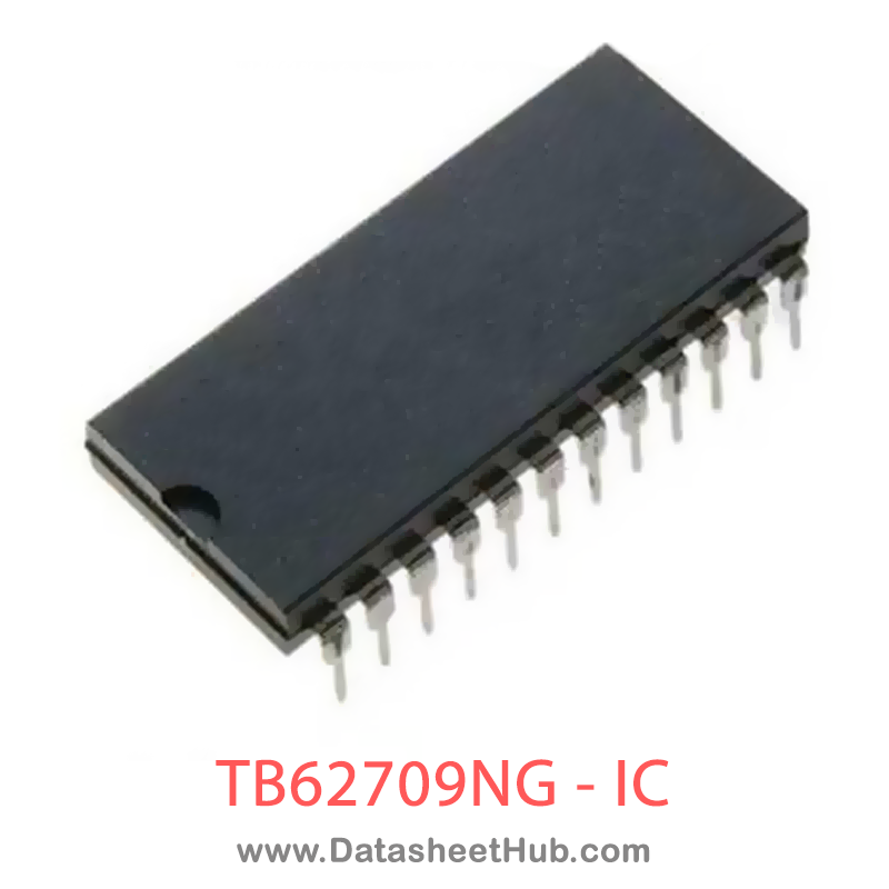
TB62709NG overview
The TB62709NG is a 7-Segment LED Display Driver With Built-In Decoders made by Toshiba, supplied in a DIP 24 Pin Type package. The absolute maximum ratings table on this page lists the 10 limits from the manufacturer's datasheet that must not be exceeded. This page brings together the TB62709NG pinout and maximum ratings, with the full datasheet PDF to preview below or download.
The TB62709NG and TB62709FG are multifunctional, compact, 7−segment LED display drivers.
These ICs can directly drive 7−segment displays and individual LEDs, and can control either a 4−digit display with decimal points, or 32 individual LEDs.
These ICs can also be used with common−anode displays. Their outputs are constant current, the ampere levels at which are set using an external resistor.
A synchronous serial port connects the IC to the CPU.
The different modes of control provided by this device including Duty Control Register Set, Digit Set, Decode Set and Standby Set, are all based on every 16−bit of serial data.
This devices are a product for the Pb free(Sn-Ag).
Datasheet
TB62709NG features
- Control circuit power supply voltage VDD = 4.5 to 5.5 V
- VDD = 4.5 to 5.5 V
- Digit output rating 17 V / −400 mA
- 17 V / −400 mA
- Decoder output rating 17 V / 50 mA
- 17 V / 50 mA
- Built−in decoder Decodes the numerals 0 to 9, certain alphabetic characters, and of course blanks code.
- Decodes the numerals 0 to 9, certain alphabetic characters, and of course blanks code.
- Digit control function Can scan digit outputs DIG−0 to DIG−3 when connected to the common anode pins of a 7−segment display.
- Can scan digit outputs DIG−0 to DIG−3 when connected to the common anode pins of a 7−segment display.
- Maximum transmission frequency fCLK = 15 MHz
- fCLK = 15 MHz
- Decoder outputs (OUT−A to OUT−Dp) Output current can be set up to a 40mA maximum using an external resistor.
- Output current can be set up to a 40mA maximum using an external resistor.
- Constant current tolerance (Ta = 25°C, VDD = 5.0 V) Variation between bits = ±7%, variation between devices (including variation between bits) = ±15% at VCE ≥ 0.7 V
- Variation between bits = ±7%, variation between devices (including variation between bits) = ±15% at VCE ≥ 0.7 V
TB62709NG pinout
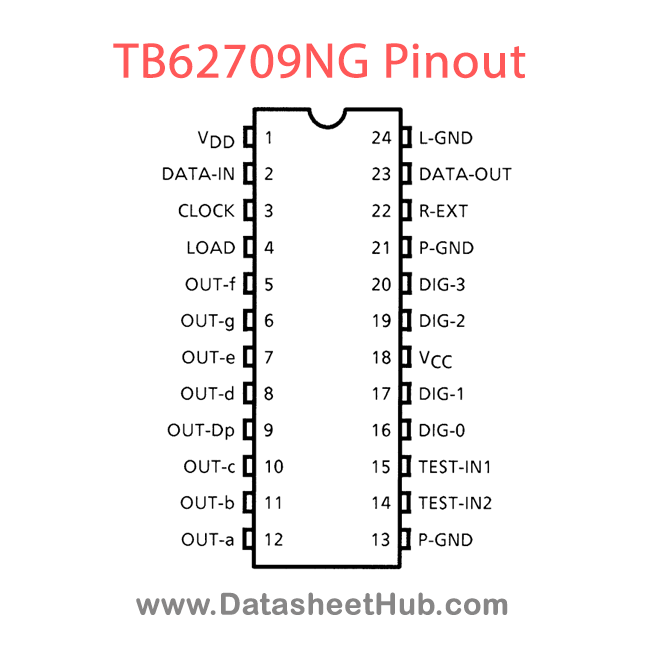
| Pin | Name | Description |
|---|---|---|
| 1 | VDD | 5 V power pin. |
| 2 | DATA−IN (DI) | Serial data input pin. |
| 3 | CLOCK (CK) | Clock input pin. The shift register shifts data on the clock's rising edge. |
| 4 | LOAD (LD) | Load signal input pin. The data in the D8 to D15 are read on the rising edge and the current load register the is selected from among the Duty Register, the Decode & Digit Register, or Data Registers 0 to 3. The D0 to D7 bits of the 16−bit shift register contain data corresponding to the same regist |
| 5~12 | OUT−A to OUT−Dp | Segment drive output pins. The A to Dp outputs correspond to the seven segments. These pins output constant sink current. Connect each of these pins to the corresponding LED's cathode. |
| 13, 21 | P−GND | Ground pins, There are two which can be used to ground the output OUT−A to OUT−Dp pins. |
| 14 | TEST−IN2 | Product test pin. In normal use, be sure to connect to ground. |
| 15 | TEST−IN1 | Product test pin. In normal use, be sure to connect to ground. |
| 16, 17, 19, 20 | DIG−0 to DIG−3 | Digit output pins. Each of these pins can control one of the four seven−segment digits in a display. These pins output the VCC pin voltage as a source current output. Connect these pins to the LED anodes. |
| 18 | VCC | Power pin for digit output. |
| 22 | R−EXT | Current setting pin for the OUT−A to OUT−Dp pins. Connect a resistor between this pin and ground when setting the current. |
| 23 | DATA−OUT (DO) | Serial data output pin. Use when TB62709N or TB62709F devices are used in cascade connections. |
| 24 | L−GND | Ground pin for logic and analog circuits. |
Absolute maximum ratings
| Parameter | Symbol | Value | Unit |
|---|---|---|---|
| Supply Voltage for Logic Circuits | VDD | 7.0 | V |
| Supply Voltage | VCC | 17 | V |
| DIG−0 to DIG−3 Output Current | IDIG | −400 | mA |
| OUT−a to Dp Output Current | IOUT | 50 | mA |
| Output Current for Logic Block | IOH / IOL | ±5 | mA |
| Input Voltage | VIN | −0.3~VDD + 0.3 | V |
| Operating Frequency | fCK | 15.0 | MHz |
| Total Supply Current | IVDD | 400 | mA |
| Operating Temperature | Topr | −40~85 | °C |
| Storage Temperature | Tstg | −55~150 | °C |
TB62709NG applications
- Automotive lighting
- LED matrix displays
- Gaming peripherals
- Industrial automation
Comments 0
Leave a comment