

TC58TEG5DCJTA00 Datasheet – Toggle DDR1.0 NAND Memory
NAND memory Toggle DDR1.0
TC58TEG5DCJTA00 overview
The TC58TEG5DCJTA00 is an NAND memory Toggle DDR1.0 made by Toshiba. The absolute maximum ratings table on this page lists the 3 limits from the manufacturer's datasheet that must not be exceeded. This page brings together the TC58TEG5DCJTA00 pinout and maximum ratings, with the full datasheet PDF to preview below or download.
Toggle DDR is a NAND interface for high performance applications which support data read and write operations using bidirectional DQS.
Toggle DDR NAND has implemented ’Double Data Rate’ without a clock. It is compatible with functions and command which have been supported in conventional type NAND(i.e. SDR NAND) while providing high data transfer rate based on the high-speed Toggle DDR Interface and saving power with separated DQ voltage. For applications that require high capacity and high performance NAND, Toggle DDR NAND is the most appropriate.
Toggle DDR1.0 NAND supports the interface speed of up to 100 MHz, which is faster than the data transfer rate offered by SDR NAND. Toggle DDR NAND transfers data at high speed using DQS signal that behaves as a clock, and DQS shall be used only when data is transferred for optimal power consumption. This device supports both SDR interface and Toggle DDR interface. When starting, the device is activated in SDR mode. The interface mode can be changed into Toggle DDR interface utilizing specific command issued by the Host.
Datasheet
TC58TEG5DCJTA00 features
- Organization
- Part number TC58TEG5DCJ TC58TEG5DCJTA00 (TOPER: 0~70℃) TC58TEG5DCJTAI0 (TOPER : -40~+85℃)
- Device capacity 17664 ´ 256 ´ 1060 ´ 8 bits
- Page size 17664 Bytes
- Block size (4M + 320 K) Bytes
- Plane size 2396651520 Bytes
- Plane per one LUN 1 Planes
- LUN per one target 1 LUNs
- Target per one device 1 targets
- Modes Basic Operation Page Read Operation (with Random Data Output), Data Out After Status Read, Sequential Cache Read Operation, Random Cache Read Operation, Page Program Operation (with Random Data Input), Cache Program Operation, Block Erase Operation, Copy-Back Program Operation (with Random Data Input), Set Feature Operation, Get Feature Operation, Read ID Operation, Read Status Operation, Re
- Basic Operation Page Read Operation (with Random Data Output), Data Out After Status Read, Sequential Cache Read Operation, Random Cache Read Operation, Page Program Operation (with Random Data Input), Cache Program Operation, Block Erase Operation, Copy-Back Program Operation (with Random Data Input), Set Feature Operation, Get Feature Operation, Read ID Operation, Read Status Operation, Reset Op
- Page Read Operation (with Random Data Output), Data Out After Status Read, Sequential Cache Read Operation, Random Cache Read Operation, Page Program Operation (with Random Data Input), Cache Program Operation, Block Erase Operation, Copy-Back Program Operation (with Random Data Input), Set Feature Operation, Get Feature Operation, Read ID Operation, Read Status Operation, Reset Operation, Reset L
- Extend Operation Page Copy (2) Operation, Device Identification Table Read Operation, Read Status Enhanced Operation, Read LUN #0 Status Operation
- Page Copy (2) Operation, Device Identification Table Read Operation, Read Status Enhanced Operation, Read LUN #0 Status Operation
- Mode control Serial input/output Command control
- Serial input/output
- Command control
- Power supply VCC = 2.7 V to 3.6 V VCCQ = 2.7 V to 3.6 V / 1.7 V to 1.95V
- VCC = 2.7 V to 3.6 V
- VCCQ = 2.7 V to 3.6 V / 1.7 V to 1.95V
- Access time
- Cell array to register 100 ms max (TENTATIVE) 50 ms typ. (TENTATIVE)
- Data Transfer rate 100 MHz
- Program/Erase time
- Auto Page Program 1400 ms/page typ. (TENTATIVE)
- Auto Block Erase 5 ms/block typ. (TENTATIVE)
- Operating current
- Read TBD mA max. (per 1 chip) Program
- (avg.) TBD mA max. (per 1 chip) Erase
- (avg.) TBD mA max. (per 1 chip)
- Standby TBD mA max. (per 1 chip)
- Package (Weight: TBD g typ.)
- (Weight: TBD g typ.)
- Reliability Refer to APPLICATION NOTES AND COMMENTS.
- Refer to APPLICATION NOTES AND COMMENTS.
TC58TEG5DCJTA00 pinout
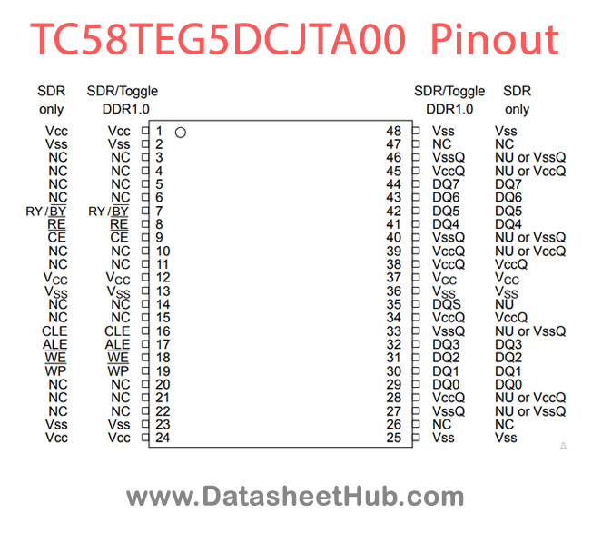
| Name |
|---|
| DATA INPUTS/OUTPUTS The DQ pins are used to input command, address and data and |
| COMMAND LATCH ENABLE The CLE input controls the activating path for commands sen |
| ADDRESS LATCH ENABLE The ALE input controls the activating path for address to t |
| CHIP ENABLE The CE input is the device selection control. When the device is in |
| READ ENABLE The RE input is the serial data-out control, and when active, drives |
| WRITE ENABLE The WE input controls writes to the DQ port. Commands, addresses ar |
| WRITE PROTECT The WP pin provides inadvertent program/erase protection during po |
| READY/BUSY OUTPUT The R/ B output indicates the status of the device operation. |
| DATA STROBE Output with read data, input with write data. Edge-aligned with read |
| POWER VCC is the power supply for device. |
| DQ POWER The VccQ is the power supply for input and/or output signals. |
| GROUND |
| DQ GROUND The VssQ is the power supply ground |
| No connection NCs are not internally connected. They can be driven or left uncon |
| Not use NUs must be left unconnected. |
Absolute maximum ratings
| Parameter | Symbol | Value | Unit |
|---|---|---|---|
| Voltage on any pin relative to VSS | VCC | -0.6 to +4.6 | V |
| VIN | VccQ(3.3V) | -0.6 to +4.6 | |
| VI/O | VccQ(3.3V) | -0.6 to +4.6 |
TC58TEG5DCJTA00 applications
- Laptops and Ultrabook
- Tablet Computers
- Memory Cards
- Embedded Systems
Comments 0
Leave a comment