

THS4531A Datasheet – Fully Differential Amplifier
Ultra Low Power, Rail-to-Rail Output, Fully-Differential Amplifier
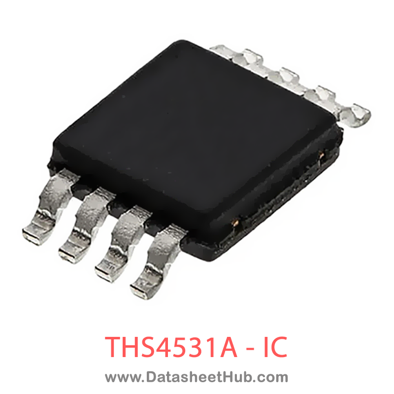
THS4531A overview
The THS4531A is an Ultra Low Power, Rail-to-Rail Output, Fully-Differential Amplifier made by Texas Instruments, supplied in these packages: SOIC,VSSOP 8 Pin Type. Main ratings: Voltage 2.5 V to 5.5 V; Current 250 µA; Power-Down Mode 0.5 µA (Typical); Bandwidth 36 MHz (Av = 1 V/V). The absolute maximum ratings table on this page lists the 8 limits from the manufacturer's datasheet that must not be exceeded. This page brings together the THS4531A pinout, key specifications and maximum ratings, with the full datasheet PDF to preview below or download.
The THS4531A device is a low-power, fully differential amplifier with input common-mode range below the negative rail and rail-to-rail output. The device is designed for low-power data acquisition systems and high-density applications where power consumption and dissipation is critical.
The device features accurate output common-mode control that allows for DC coupling when driving analog-to-digital converters (ADCs). This control, coupled with the input common-mode range below the negative rail and rail-to-rail output, allows for easy interface from single-ended ground-referenced signal sources to successive-approximation registers (SARs), and delta-sigma (ΔΣ) ADCs using only single-supply 2.5-V to 5-V power. The THS4531A is also a valuable tool for general-purpose, low-power differential signal conditioning applications.
Key specifications
Datasheet
THS4531A features
- Ultra Low-Power: Voltage: 2.5 V to 5.5 V Current: 250 µA Power-Down Mode: 0.5 µA (Typical)
- Fully Differential Architecture
- High DC Accuracy: VOS: ±100 µV VOS Drift: ±3 µV/˚C (–40°C to +125°C) AOL: 114 dB
- Rail-to-Rail Output (RRO)
- Negative Rail Input (NRI)
- Output Common-Mode Control
- 8-Pin SOIC (D) and VSSOP (DGK)
- 10-Pin WQFN (RUN)
THS4531A pinout
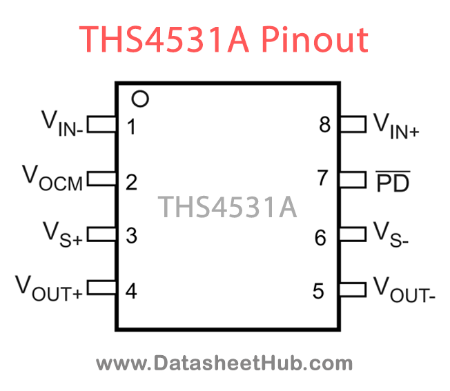
| Name | Description |
|---|---|
| NC | No internal connection |
| 8 | |
| PD | Power-down, PD = logic low = low power mode, PD = logic high = normal operation (PIN MUST BE DRIVEN) |
| VIN+ | Non-inverted amplifier input |
| VIN– | Inverting amplifier input |
| VOCM | Common-mode voltage input |
| VOUT+ | Non-inverted amplifier output |
| VOUT– | Inverted amplifier output |
| VS+ | Amplifier positive power-supply input |
| VS– | Amplifier negative power-supply input. On multichannel devices, VS– is tied together. |
Absolute maximum ratings
| Parameter | Value | Unit |
|---|---|---|
| Supply voltage, VS– to VS+ | Min 5.5 | |
| Input/output voltage, VIN±, VOUT±, and VOCM pins | Min (VS–) – 0.7 / Max (VS+) + 0.7 | V |
| Differential input voltage, VID | Min 1 / Max V | |
| Continuous output current, IO | Min 50 / Max mA | |
| Continuous input current, Ii | Min 10 / Max mA | |
| Maximum junction temperature, TJ | Min 150 / Max °C | |
| Operating free-air temperature, TA | Min –40 / Max 125 | °C |
| Storage temperature, Tstg | Min –65 / Max 150 | °C |
THS4531A applications
- Low-Power SAR, ΔΣ ADC Driver
- Low-Power, High Performance
- Differential-to-Differential Amplifier
- Single-Ended to Differential Amplifier
- Low-Power, Wide-Bandwidth Differential Driver
- Low-Power, Wide-Bandwidth Differential Signal Conditioning
- High-Channel Count and Power Dense Systems
Comments 0
Leave a comment