
uP6103S8 Datasheet – Synchronous-Rectified Buck Controller
5V/12V Synchronous-Rectified Buck Controller with Reference Input
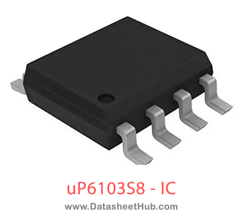
uP6103S8 overview
The uP6103S8 is a 5V/12V Synchronous-Rectified Buck Controller with Reference Input, supplied in an SOP-8L Type package. The absolute maximum ratings table on this page lists the 10 limits from the manufacturer's datasheet that must not be exceeded. This page brings together the uP6103S8 pinout and maximum ratings, with the full datasheet PDF to preview below or download.
The uP6103 is a compact synchronous-rectified buck controller specifically designed to operate from 5V or 12V‘supply voltage and to deliver high quality output voltage as low as 0.4V. These SOP-8 and PSOP-8 devices operate at fixed 200/300 kHz frequency and provide an optimal level of integration to reduce size and cost of the power supply. The UP6103 supports both tracking mode and stand-alone mode operation. The output voltage s tightly regulated to the external reference voltage from 0.4V t0 3.0V at tracking mode or to internal 0.6V reference at stand-alone mode. This controller integrates internal MOSFET drivers that support 12V+12V bootstrapped voltage for high efficiency power conversion. The bootstrap diode is built-in to simplify the circuit design and minimize external part count. Other features include internal soft start, undervoltage protection, overcurrent protection and shutdown function. With aforementioned functions, this part provides customers a compact, high efficiency, well-protected and cost effective solutions. This part is available in SOP-8 andPSOP-8 packages.
Datasheet
uP6103S8 features
- Operate from 5V or 12V Supply Voltage
- 3.3V10 12V V,, Input Range
- 0.6V,,, with 1.5% Accuracy
- Output Range from V,, o 80% of Vin
- Support Tracking Mode and Stand Alone Mode Operation
- Simple Single-Loop Control Design Voltage-Mode PWM Control Fast Transient Response
- Voltage-Mode PWM Control
- Fast Transient Response
- High-Bandwidth Error Amplifier 0% t0 80% Duty Cycle
- 0% t0 80% Duty Cycle
- Lossless, Programmable Overcurrent Protection Uses Lower MOSFETR,,,
- Uses Lower MOSFETR,,,
- 200/300 kHz Fixed Frequency Oscillator
- Internal Soft Start
- Integrated Bootstrap Diode
- RoHS Compliant and Halogen Free
uP6103S8 pinout
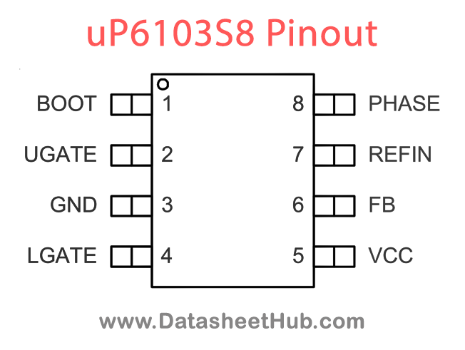
| Pin | Name | Description |
|---|---|---|
| 1 | BOOT | Bootstrap Supply for the floating upper gate driver. Connect the bootstrap capacitor CBOOT between BOOT pin and the PHASE pin to form a bootstrap circuit. The bootstrap capacitor provides the charge to turn on the upper MOSFET. Typical values for CBOOT range from 0.1uF to 0.47uF. Ensure that CBOOT i |
| 2 | UGATE | Upper Gate Driver Output. Connect this pin to the gate of upper MOSFET. This pin is monitored by the adaptive shoot-through protection circuitry to determine when the upper MOSFET has turned off. |
| 3 | GND | Signal and Power Ground for the IC. All voltages levels are measured with respect to this pin. Tie this pin to the ground island/plane through the lowest impedance connection available. |
| 4 | LGATE | Lower Gate Driver Output. Connect this pin to the gate of lower MOSFET. This pin is monitored by the adaptive shoot-through protection circuitry to determine when the lower MOSFET has turn off. |
| 5 | VCC | Supply Voltage. This pin provides the bias supply for the uP6103 and the lower gate driver. The supply voltage is internally regulated to 4VDD for internal control circuit. Connect a well-decoupled 4.5V to 13.2V supply voltage to this pin. Ensure that a decoupling capacitor is placed near the IC. |
| 6 | FB | Feedback Voltage. This pin is the inverting input to the error amplifier. A resistor divider from the output to GND is used to set the regulation voltage. Use this pin in combination with the COMP/EN pin to compensate the voltage control feedback loop of the converter. |
| 7 | REFIN | External Reference Input for Tracking Mode Operation. This pin receives a voltage with range from 0.4V to 3.0V as the reference voltage at the non-inverting input of the error amplifier. Pulling this pin lower than 0.3V disables the controller and causes the oscillator to stop, the UGATE and LGATE o |
| 8 | PHASE | PHASE Switch Node. Connect this pin to the source of the upper MOSFET and the drain of the lower MOSFET. This pin is used as the sink for the UGATE driver, and to monitor the voltage drop across the lower MOSFET for over current protection. This pin is also monitored by the adaptive shoot-through pr |
| Exposed Pad | For PSOP-8 package. The exposed pad should be well soldered to PCB for effective |
Absolute maximum ratings
| Parameter | Value |
|---|---|
| Supply Input Voltage, VCC (Note 1) | -0.3V to +15V |
| PHASE to GNDDC < 200ns | -5V to 15V-10V to 30V |
| BOOT to GNDDC< 200ns | -0.3V to PHASE +15V -0.3V to 42V |
| LGATE to GNDDC< 200ns | -1V to 15V -5V to 30V |
| UGATE to PHASEDC< 200ns | -0.3V to 15V-2V to 20V |
| Input, Output or I/O Voltage | -0.3V to +6V |
| Storage Temperature Range | -65OC to +150OC |
| Junction Temperature | 150OC |
| Lead Temperature (Soldering, 10 sec) | 260OC |
| ESD Rating (Note 2) HBM (Human Body Mode) MM (Machine Mode) | 2kV 200V |
uP6103S8 applications
- Power Supplies for Microprocessors or Subsystem Power Supplies
- Cable Modems, Set Top Boxes, and xDSL Modems
- Industrial Power Supplies; General Purpose Supplies
- 5V or 12V Input DC-DC Regulators
- Low Voltage Distributed Power Supplies
Comments 0
Leave a comment